Abstract
In order to ensure good charging performance of new energy vehicles, the charging station was designed and the relevant oscillation circuits were optimized. The function and structure of the charging station was determined, and through a hierarchical framework, not only the success rate factor could be corrected, but also a resonant converter was combined to achieve efficient charging over a wide battery voltage range. The linear charging management chip was adopted, which integrated high-precision constant voltage source, temperature monitoring, charging status display, and battery charging completion termination function. The changes in excitation current and switching frequency during the charging process were studied, and the optimization basis for the relevant circuits was determined. A trigger was added to the input end of the oscillator to filter the input signal, which improved the accuracy of the RC oscillator cycle. The clock reference oscillation circuit and stable voltage power supply circuit were optimized. In order to verify the effectiveness of the proposed electronic control design, a hardware platform for the test of DC output characteristics was built. The results indicate that the output voltage waveform can effectively meet the working requirements.
Highlights
- The linear charging management chip was adopted, which integrated high-precision constant voltage source, temperature monitoring, charging status display, and battery charging completion termination function.
- A trigger was added to the input end of the oscillator to filter the input signal, which improved the accuracy of the RC oscillator cycle.
- In order to verify the effectiveness of the proposed electronic control design, a hardware platform for the test of DC output characteristics was built.
1. Introduction
The power batteries in new energy vehicles are charged using specific interfaces from external power sources through AC or DC charging systems [1]. Therefore, the performance of the charging station has a critical impact on charging efficiency, battery life, and so on, especially the stability during the charging process [2, 3]. The AC charging system is usually an on-board charger installed inside an electric vehicle. The on-board charger is powered by an external AC power grid. The DC charging system is usually installed at a fixed charging station, which directly sends the adjusted output current to the power battery, and is usually used in fast charging situations. DC charging stations are often installed in a fixed location, such as a garage or specialized charging station. This type of DC charging station uses a dedicated charging line, which can output higher power to accelerate charging speed. Because the output of the charging station is DC and different power battery systems correspond to different battery voltages, different cars correspond to different DC outputs. Modern charging stations have a system specifically designed to detect battery voltage and adjust output [4]. During the rapid charging process, the circuit is prone to significant oscillation issues, which have a strong impact on the battery and need to be studied and improved [5, 6]. By designing charging stations and optimizing oscillation circuits, the safety and stability of new energy vehicles can be further ensured.
2. Overall design of charging station
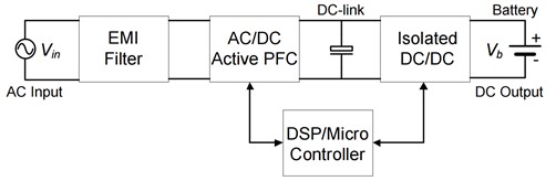
2.1. Design of overall structure and function
Single phase active PFC technology is mainly divided into single stage and two-stage. Single stage active PFC is only suitable for low-power applications. In addition, due to the presence of a large number of low-frequency ripple in the output current, this single-stage PFC is only used for lead-acid batteries. Electrical isolation is also a major safety requirement for protecting electric vehicle users in on-board chargers, so two-stage on-board chargers are currently the mainstream solution. The two-stage on-board charger often has an active PFC circuit in the front stage and an isolated DC/DC circuit in the back stage. The overall structure of the designed charging station is shown in Fig. 1. The front stage PFC circuit rectifies AC into a high-voltage DC bus and achieves power factor correction. The later isolated DC/DC converts the high-voltage DC bus into the required charging voltage to charge the lithium battery pack, further regulating the voltage pulsation of the high-voltage bus to prevent low-frequency pulsation in the bus voltage from being transmitted to the battery side.
Fig. 1Overall design of charging station
2.2. Design of control chip
The designed chip is a typical linear charging management chip, as shown in Fig. 2.
Fig. 2Wiring diagram of control chip
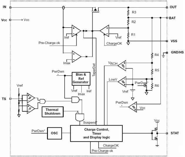
This chip provides integrated success rate field-effect transistors, high-precision constant voltage sources, temperature monitoring, charging status display, and battery charging completion termination functions. When the chip charges the battery, the charging current is limited, rather than operating under constant current charging. The pre charging stage with time constraints is used to pre charge deeply discharged batteries. Once the battery voltage reaches the charging voltage, the high-precision constant voltage charging stage will start and complete the entire charging process. The chip terminates charging by minimizing the current. In addition, the chip also includes a low-power sleep mode, which means that when the power supply voltage VCC is lower than the battery voltage, the chip enters sleep mode. When the battery voltage is lower than VRCH, the recharging process will be initiated.
2.3. Control of excitation response
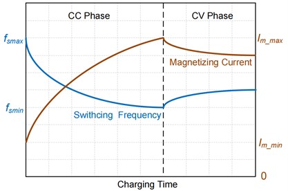
In order to obtain the open-circuit voltage curve, the battery is charged and discharged at a constant current of 8 A, continuously recording the ampere hours of the battery and the corresponding battery voltage. The measured voltage data is transmitted to the upper computer through CAN communication using BMS. The variation curve of the excitation current during the charging process is shown in Fig. 3. It can be seen that as the charging progresses, the battery voltage gradually increases and the switching frequency gradually decreases, resulting in a significant increase in the excitation current. Excessive excitation current will increase the conduction and turn off losses of the switch tube. So it is necessary to consider the optimization design of excitation current. The process of constant current and constant voltage charging is mainly divided into two stages. Firstly, the battery is charged with a constant current until it is charged to 70 % to 90 % of the stage. After the battery voltage reaches the preset value, the constant current mode switches to the constant voltage mode. Then charge the battery with a constant voltage, and the charging current gradually decreases. Even if the constant voltage mode is only used for the small remaining capacity of the charging pool, this stage still needs to take up a certain amount of time, because the constant voltage charging stage of the battery is a process where the charging current gradually decreases to zero.
Fig. 3The variation curve of excitation current and switching frequency during the charging process
3. Analysis of circuit oscillation characteristics
3.1. Optimization of clock reference oscillation circuit
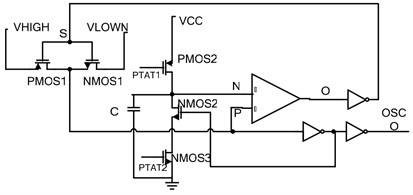
The main problem to be overcome at present is the impact of changes in power supply voltage on the accuracy and amplitude of the oscillator. The main reason why RC oscillators are not stable and have low accuracy is that their level flipping is closely related to the jump in power supply voltage. If two signals are used for error comparison, as both signals are affected by changes in power supply voltage, the influence of power supply voltage can be eliminated or partially eliminated during error comparison, thereby stabilizing the waveform of the oscillator. Another reason for the low accuracy of traditional RC oscillators is that their period mainly depends on the product of RC. In order to improve accuracy, the period of the oscillator can be mainly determined by the delay time of the error comparator, and the charging and discharging time of RC is determined by the charging and discharging current. If the charging and discharging current can be controlled, a relatively high accuracy oscillator circuit can be obtained. According to the optimized design, the circuit architecture diagram of the oscillation module generated by the clock reference can be obtained as shown in Fig. 4. The circuit undergoes two processes of capacitor charging and discharging to achieve oscillation. VHIGH and VLOWN are at “1” and “0” levels. When the S-terminal is high or low, the high and low levels are alternately selected for output, becoming the output of the oscillator.
Fig. 4Design of clock reference oscillation circuit
3.2. Optimization of stable voltage power supply circuit
According to the overall requirements of chip design, the regulated power module must generate a series of reference voltages that are minimally affected by the power supply voltage, temperature, and process angle. Since the highest required reference voltage is 4.2 V, while the output voltage of a typical bandgap reference generation circuit is 1.25 V or 2.5 V, a low voltage differential linear regulator needs to be designed to obtain the required reference level. Although the co emission amplifier circuit has Miller effect, its speed can be improved by setting a lower gain for it. The second stage amplification circuit is the main amplification stage of the operational amplifier, which is achieved by setting a larger resistance value. Due to the absence of Miller effect in the common base amplifier circuit, it can achieve high gain while also considering high speed. So the operational amplifier has a high speed, which will greatly shorten the response time of the reference voltage under various interferences. The optimized and simplified regulated power supply circuit is shown in Fig. 5. Due to the two-stage operational amplifier, capacitors are used as Miller compensation to ensure loop stability. Constant current charging is a charging strategy that maintains a constant current flowing into the battery by changing the charging voltage. When the charging voltage reaches a preset value, charging stops. On the contrary, during constant voltage charging, the charging voltage is kept constant and the charging current is changed until the charging current decreases to near zero. Constant power charging refers to maintaining a constant power during charging, as the battery can be seen as a voltage source. Therefore, this method is somewhat similar to constant voltage charging, except that the charging current does not change relatively much. Reduced current charging is achieved through an uncontrolled voltage source, and as the battery voltage increases, the charging current decreases in an uncontrolled manner. Due to the fact that reduced current charging is not regulated, it can easily lead to overcharging and cause harm to the battery.
In order to verify the effectiveness of the proposed electronic control design, a hardware platform for the test of DC output characteristics was built in the laboratory, as shown in Fig. 6. The charging module consists of 20 lithium batteries, with a single rated voltage of 3.6 V and a rated capacity of 200 Ah. The resonant inductance of the charger consists of two parts, one of which is an independent inductance wound on the magnetic core 25 μH. The other part is the leakage inductance of the transformer 12 μH. The total resonant inductance is 37 μH. The adjustment range of switch frequency is from 80 kHz to 120 kHz. The digital control chip used is STM32F103R8T6.
Fig. 5Optimized and simplified regulated power supply circuit
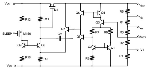
Fig. 6Hardware platform for the test of DC output characteristics
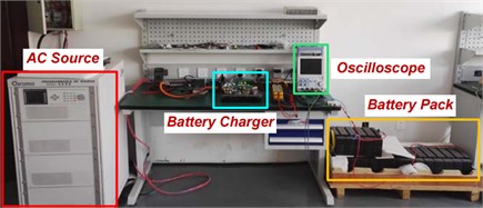
a) Hardware architecture
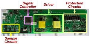
b) Composition of the controller
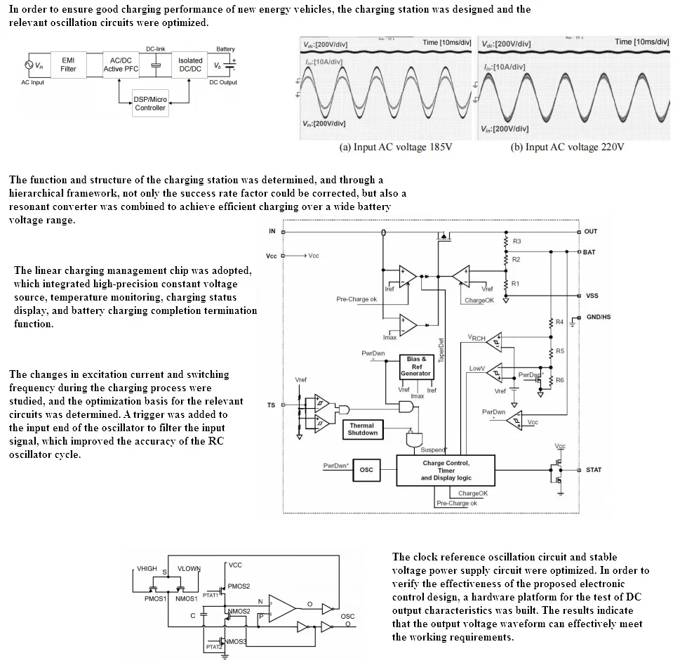
Under the conditions of input AC voltage of 185 V and 220 V, the DC output voltage waveform was tested, as shown in Fig. 7. and represent the input AC voltage and current, respectively, is the DC output voltage. It can be seen that the voltage under different sampling numbers has good stability, and the output deviation is very low, which can effectively meet the requirements. Under different input conditions, the stability of the DC output voltage is good and there is no oscillation problem. When the battery voltage reaches constant voltage VOREG, it will enter a constant voltage charging state. Within the entire operating temperature and voltage range, the constant voltage accuracy is higher than 0.5 %, and the chip monitors the battery voltage through BAT and VSS pins. For safety reasons, a safety timer is also designed during the constant voltage charging phase. During the charging process, if the timer counts but the battery is not fully charged, the chip turns off power FET, stops charging, and indicates an error on the STAT pin. The error mode is eliminated by repowering on the power or reinserting the battery.
Fig. 7Output voltage waveform
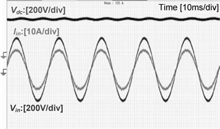
a) Input AC voltage 185 V
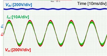
b) Input AC voltage 220 V
4. Conclusions
The key to sustainable development of electric vehicles lies in continuously improving their performance to ensure their core competitiveness. At present, the main development trends of electric vehicle technology are transmission systems, battery systems, and charging devices. In terms of research on charging devices, the following conclusions can be drawn:
1) In the constant voltage charging stage, charging management requires the output of a constant voltage, which is not only a requirement for accuracy, but also relates to the safety of charging. A high-precision reference voltage source has become an important task, and the core of the voltage source is the bandgap reference.
2) When making error comparisons, the influence of power supply voltage can be eliminated or partially eliminated, thereby stabilizing the waveform of the oscillator. In order to improve accuracy, the period of the oscillator can be mainly determined by the delay time of the error comparator, and a relatively high precision oscillator circuit can be obtained.
References
-
O. O. Ademulegun, P. Macartain, B. Oni, and N. J. Hewitt, “Multi-stage multi-criteria decision analysis for siting electric vehicle charging stations within and across border regions,” Energies, Vol. 15, No. 24, p. 9396, Dec. 2022, https://doi.org/10.3390/en15249396
-
Y. An, Y. Gao, N. Wu, J. Zhu, H. Li, and J. Yang, “Optimal scheduling of electric vehicle charging operations considering real-time traffic condition and travel distance,” Expert Systems with Applications, Vol. 213, No. 1, p. 118941, Mar. 2023, https://doi.org/10.1016/j.eswa.2022.118941
-
D. Keith and J. Womack, “Building and sustaining reliable public EV charging in the United States,” Environmental Research Letters, Vol. 18, No. 1, p. 011004, Jan. 2023, https://doi.org/10.1088/1748-9326/acae39
-
K. Drobnic et al., “An output ripple-free fast charger for electric vehicles based on grid-tied modular three-phase interleaved converters,” IEEE Transactions on Industry Applications, Vol. 55, No. 6, pp. 6102–6114, Nov. 2019, https://doi.org/10.1109/tia.2019.2934082
-
S. V. Matsievskiy and V. I. Kaminskii, “Autogenerator with ferrite circulator powered hybrid electron accelerator characteristics modeling,” Physics of Atomic Nuclei, Vol. 84, No. 10, pp. 1748–1751, Dec. 2021, https://doi.org/10.1134/s1063778821100252
About this article

The paper is supported by the “Science and Technology Innovation China” project in Yantai City in 2022, titled “Research on the Layout and Planning of New Energy Vehicle State Grid Charging Stations in Yantai City Based on Big Data”.
The datasets generated during and/or analyzed during the current study are available from the corresponding author on reasonable request.
The authors declare that they have no conflict of interest.
