Abstract
Precise microstructures find their application in various areas: laser industry; electronic, microfluidic devices. There are several processes for production of precise periodic microstructures. One of these processes is hot imprint, on the other hand there are many challenges, related with quality of microstructure. One of the solutions for the quality issues is exploitation of ultrasonic excitation during the process of mechanical hot imprint. In the paper analytical measures and analysis algorithms for the measurement of quality parameters of already created microstructure, as well for dynamic analysis of created vibroactive pad are presented. In the end of the paper vibroactive pads are experimentally analysed using already discussed equipment and measuring algorithms, in order to find out their operating frequencies.
1. Introduction
David Rittenhouse, an American astronomer, made the first periodical microstructure in 1785 [1]. It is reported that the microstructure was half inch-wide. It was not as small as microstructures, created by novel technologies, but this was the beginning of invention. From 1785 periodical microstructure changed in size and manufacturing ways, but the whole concept remained the same. The microstructure is composed from narrow grooves separated by spaces between them, which are in the level of propagating light’s wavelength.
Nowadays science is more concerned on micro and nano levels of our surrounding world. Scientists are establishing new ways of using common physical phenomena for achieving new inventions or improving already existing solutions [1-48]. To do so, micro scientific equipment has to be constructed and exploited in order to achieve previously stated objectives.
Scientific equipment used for nano or micro levels of measurements mainly consists of micro-mechanical systems. Furthermore, a periodical microstructure has a great role in these micro-mechanical systems. Periodical microstructures are being used in lasers, sensors, holography, etc.
A periodical microstructure is constructed of narrow grooves separated by spaces between them which are in the level of propagating light’s wavelength. With the help of periodical microstructure, the propagating polychromatic light can be separated into its components. Furthermore, the number of components depends on the period of the microstructure and propagating light which can be transmitted or reflected. These components then become the foundation of analysis because transforms in to monochromatic light.
By mentioning nano levels, one can bear in mind very small material and the quality it has to reach to be sufficient in providing good efficiency and worth of the experiment. In order to achieve good quality of periodical microstructures, precise processing regimes have to be maintained throughout the manufacturing of this microstructure.
In this paper experimental techniques, analysis of periodic microstructures and vibroactive pads, whose purpose is improvement the quality of periodical microstructures, created during mechanical hot imprint, of two different constructions are presented.
2. Polycarbonate used for replication of periodical microstructures
The application of polycarbonate (Fig. 1) in replication of periodical microstructures was analyzed by Janušas G. and Narijauskaitė B. in 2013. It is stated that polycarbonate is a suitable material for periodical microstructure’s replication because of its physical properties, such as [49]:
• Strength;
• Ability to withstand scratches;
• Easily cleaned;
• Usability in high temperatures.
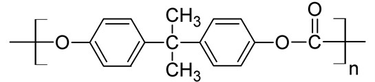
Fig. 1Chemical formula of polycarbonate
The thermal, chemical and physical properties of polycarbonate are shown in the Table 1-Table 3.
Table 1Thermal properties of polycarbonate
Melting temperature () | 267°C |
Glass transition temperature () | 150°C |
Heat deflection temperature – 10 kN | 145°C |
Heat deflection temperature 0.45 MPa | 140°C |
Heat deflection temperature – 1.8 MPa | 128-138°C |
Upper working temperature | 115-130°C |
Lower working temperature | –40°C |
Linear thermal expansion coefficient | 65-70×10-6/K |
Specific heat capacity | 1.2-1.3 kJ/(kg∙K) |
Thermal conductivity 23°C | 0.19-0.22 W/(m∙K) |
Table 2Chemical properties of polycarbonate
Young’s modulus | 2.0-2.4 GPa |
Tensile strength | 55-75 MPa |
Compressive strength | >80 MPa |
Poisson’s ratio | 0.37 |
Coefficient of friction | 0.31 |
Table 3Physical properties of polycarbonate
Density | 1.20-1.22 g/cm3 |
Refractive index | 1.584-1.586 |
Water absorption - Equilibrium | 0.16-0.35 % |
Water absorption – over 24 hours | 0.1 % |
Light transmittance | 88 % |
3. No contact holographic measure-system PRISM
By introducing high frequency vibrations in the thermal embossing fabrication method a difficulty of measuring these vibrations occur. Because of very high frequency, the amplitude of these vibrations seeks only the level of micrometers and they are impossible to be seen by naked eye. For measuring this kind of dynamic processes, the most efficient and suitable method is digital holographic interferometry [50, 51].
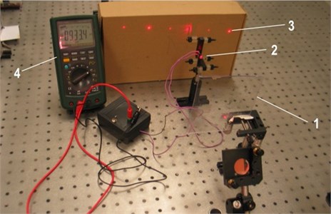
Kaunas University of Technology has a no-contact holographic measure-system PRISM. This equipment is bought from USA manufacturer HYTEC. The system consists of a control block, illumination head of the object and video camera (Fig. 2).
For analysis, PRISM uses green color light beam (532 nm). The beam from control block through fiber is directed to the lens systems where it is expanded and directed to the object. The supporting beam through fiber goes to video camera where it interferes with registered beam which is reflected from the object. With the help of video camera and control block, the ratio between object beam and supported beam until the best interference zones, can be seen. The interference view is sent to the computer, where with the help of PRISMA-DAQ software, it is processed. User can see the dynamical processes in the screen (Fig. 3) [41]. The generated view of a dynamical structure can be seen in the Fig. 4.
The specification of holographic measuring system PRISM can be found in Table 4.
Fig. 2No contact holographic measure-system PRISM: 1 – control block, 2 – illumination head of object, 3 – video camera [41]
![No contact holographic measure-system PRISM: 1 – control block, 2 – illumination head of object, 3 – video camera [41]](https://static-01.extrica.com/articles/15911/15911-img2.jpg)
Table 4Specifications of holographic measuring system PRISM
Measurement Sensitivity | < 20 nm |
Dynamic Range | 10 µm |
Measurement Range | > 100 µm |
Largest Part Size | 1 meter diameter |
Working Distance | > ¼ meter |
Data Acquisition Rate | 30 Hz |
Laser | 20 mV |
Fig. 3PRISM system’s setup [53]
![PRISM system’s setup [53]](https://static-01.extrica.com/articles/15911/15911-img3.jpg)
Fig. 4A hologram of a dynamical structure by 4700 Hz 40 V signal excitation [4]
![A hologram of a dynamical structure by 4700 Hz 40 V signal excitation [4]](https://static-01.extrica.com/articles/15911/15911-img4.jpg)
4. Diffractometer
Optical investigation setup and simplified scheme, used in order to determine diffraction efficiencies are shown in Fig. 5 and Fig. 6, consists of three major parts: sample, photodiode, and ammeter. The laser ( 632.8 nm) and photodiode BPW-34 were used in order to measure diffraction efficiency. Scheme is connected to tester.
In order to eliminate material optical properties and evaluate the geometry, the relative diffraction efficiency () is calculated by using following formulas:
where – intensity of diffraction maxima of th reflection under the th angle of illumination; – sum of all intensities of diffraction maxima under the th angle of illumination.
Fig. 5Measurement of diffraction efficiency: 1 – sample, 2 – photodiode, connected to ammeter, 3 – distribution of diffraction maxima, 4 – ammeter
The current, which passes through photodiode, is being registered by the ammeter. The magnitude of the current is directly proportional to the amounts of photons of the light, which strike the photodiode. According to the Eq. (2), sum () of all currents (different diffraction angles) is being calculated and then particular current (value of particular maxima) is being divided from this sum and the relative value (%) of diffraction efficiency is thus obtained. The most important indicator in practice, which determines optical quality of the grating, is +1 and –1 maxima. This property (bigger diffraction efficiency value of these maxima) is strongly desirable in various applications [54].
In this Master Thesis the whole replication process with its regimes was analyzed, therefore all of maxima were taken into consideration. By comparing whole array of maxima one can find how well the microstructure is replicated as a whole and not only two maxima points.
Fig. 7Main window of GSolver (default parameter window)
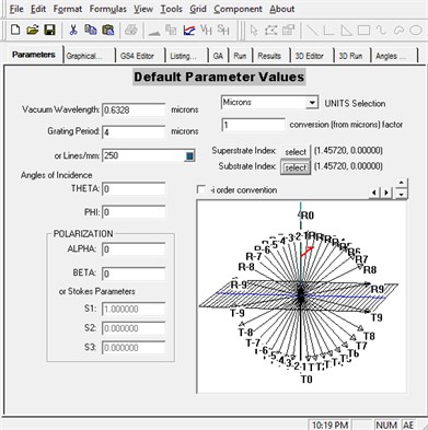
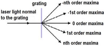
Fig. 6Simplified scheme of distribution of diffraction maxima
5. GSolver modeling software
GSolver (Fig. 7) was created by Grating Solver Development Company in 1994. This tool has enabled to model transmission and refraction diffraction efficiencies for multilayered, variable thickness, depth and profile geometry periodical microstructures.
The calculation tool for this software is based on modal or coupled-wave method (Fig. 8). The simulation of diffracted electromagnetic wave’s fields, phases and diffraction efficiencies from selected microstructure is taken for every layer of the periodical microstructure separately. Afterwards, all the solutions are combined and boundary conditions are introduced [55].
Fig. 8Periodical microstructure’s and propagating light’s scheme [56]
![Periodical microstructure’s and propagating light’s scheme [56]](https://static-01.extrica.com/articles/15911/15911-img8.jpg)
RCW (Rigorous Couple-Wave) algorithm is easily adaptable. All the calculations are done only by one period. The periodical microstructure is approximated by layers in the interval (here, – the period of a periodical microstructure). During the modeling, it is taken that the ambient of model is homogeneous, linear and isotropic [55, 56].
Maxwell’s equation is adapted to this model with boundary and Rayleigh-Jeans radiant law conditions (Eq. (3)):
where, is the incident reflected diffracted and transmitted diffracted fields (depending on the needed solution); is the dielectric permittivity [55, 56, 57].
The most accurate method is called integral method. It allows analyzing periodical microstructure diffraction efficiencies in all spectral range. Here, the profile, without non approximated Furje series, but which fully defines the real profile of the microstructure is integrated taken in mind the profile changes and the first derivative of the series. With this method, it is possible to calculate diffraction efficiencies, when structures have micro roughness.
Diffraction efficiency is calculated with Eq. (4), like closed surface Helmholtz – Kirchhoff integral:
here, – coordinate of the profile, which is equivalent to the rectangular coordinates and , - cyclic frequency, – vacuum permeability, – current in profile lengths unit in plane, perpendicular to this profile, Dirac delta function is equal to one, when and , other times, it is equal to zero, – solution of Helmholtz inequality [58].
Integration through profile can be replaced by integration through one period when the incident wave’s kvazi-periodicity is assessed. Then, Eq. (4) can be rewritten as infinite integral sum. Here, the Gryn’s functions can be defined as consistent expansions of plane wave:
here, and – vector component of the wave, – function, which defines surface on plane , – period of microstructure, – angle of irradiance (in respect of axis), – depth of microstructure, – surface normal vector. With this method, integration of only one period segment compiles to integration of whole surface [58].
6. Ultrasonic thermal embossing setup
To understand the whole ultrasonic thermal embossing process, step by step procedure has to be known. This procedure can be found in the following list:
1) Preheating of plate with master mold;
2) Pressing a rigid mould with the required pattern of features into the softened material. Here the pattern is negative. At the same moment the vibroactive pad is generating high frequency vibrations;
3) When the heating plate reaches the softened material it presses down for 0.5 s, till the pressure reaches nominal value and later nominal pressure is held for required time;
4) Releasing the mold.
In Fig. 9 the schematic diagram of ultrasonic thermal embossing can be seen.
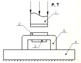
Fig. 9. The schematic diagram of ultrasonic thermal embossing: 1 – the head of the press; 2 – formable material (polycarbonate); 3 – the piezoelectric material; 4 – the base of the tool; 5 – the vibrating platform [41]
The piezoelectric material excites high frequency vibrations which with the help of aluminum vibrating platform are being transferred to the polycarbonate. The piezoelectric material and vibrating platform makes one element – vibroactive pad.
7. Master periodical microstructure
In this work, the replicas of periodical microstructures will be analyzed. In order to fabricate these replicas, the master periodical microstructure is required. By using the master periodical microstructure, it is possible to fabricate all the replicas with the desired process regimes.
The master microstructure used in this work was made of Nickel. It had 4 µm period (the land and the ridge are equal – 2 µm) and 300 µm depth (Fig. 10).
The realistic view of a master microstructure can be seen in Fig. 11. The picture was made with atomic force microscope.
Master microstructure was used not only for fabrication of microstructure replicas but also for analyzing what diffraction efficiencies could be obtained having an ideal replica. With the help of GSolver software, the ideal replica was modeled and all fabricated replicas were compared to these results.
Fig. 10Schematic drawing of master periodical microstructure
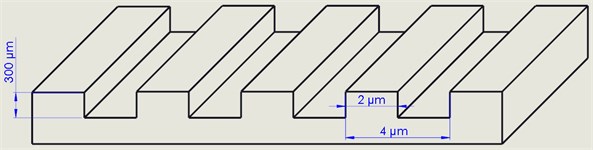
Fig. 11The view of master periodical microstructure done with atomic force microscope
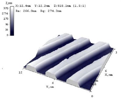
Table 5Properties of PZT-4 material
General | |
Density (103 kg/m3) | 7.5 |
Curie temperature (K) | 601 |
Elastic constants | |
(GPa) | 139 |
(GPa) | 115 |
(GPa) | 77.8 |
(GPa) | 74.3 |
(GPa) | 25.6 |
(GPa) | 30.6 |
Piezoelectric constants | |
(C/m2) | –5.2 |
(C/m2) | 15.1 |
(C/m2) | 12.7 |
Dielectric constants | |
(10-9 F/m) | 6.461 |
(10-9 F/m) | 5.620 |
8. Vibroactive pad and replication process regimes
It has been shown, that thermal embossing replication provides low quality periodical microstructures [26, 28-29]. To eliminate these faults high frequency vibrations created by a vibrating pad are introduced in the replication process.
In 2013 Kaunas University of Technology team constructed the vibrating pad to excite the high frequency vibrations to the polycarbonate in order to increase the quality of periodical microstructures. The vibrating pad or vibroactive pad is made of aluminum cylinder and a ring of piezoelectric material. The piezoelectric material is excited to produce a vibrational response. The piezoelectric element selected was PZT-4. Its properties are shown in Table 5.
The created vibrating platform was selected to have cylinder geometry with dimensions as following: 50 mm external diameter ring; 20 mm internal diameter and 2 mm thickness (Fig. 12). It was made of aluminum.
The technical drawing of the vibrating platform can be seen in the Fig. 13.
In 2014, the vibroactive pad was improved. This generation of vibroactive pad has a stack type piezoactuator instead of piezoelectric ring. A stack type piezoactuator model PSt 150/4/20 VS9 (Fig. 14) was chosen, because of actuator that is able to generate vibrations of higher amplitude. The technical drawing of this vibroactive pad can be seen in Fig. 15. From the technical drawing one can see that the thickness of vibrating platform is 1 mm.
The 1st generation vibroactive pad and the 2nd generation vibroactive pad in real life form can be seen in Fig. 16.
Fig. 12The 3D view of the vibration platform (A) and the vibration platform (1) with the piezoelectric element (2) attached [41]
![The 3D view of the vibration platform (A) and the vibration platform (1) with the piezoelectric element (2) attached [41]](https://static-01.extrica.com/articles/15911/15911-img12.jpg)
![The 3D view of the vibration platform (A) and the vibration platform (1) with the piezoelectric element (2) attached [41]](https://static-01.extrica.com/articles/15911/15911-img13.jpg)
Fig. 13The drawing of the vibration platform
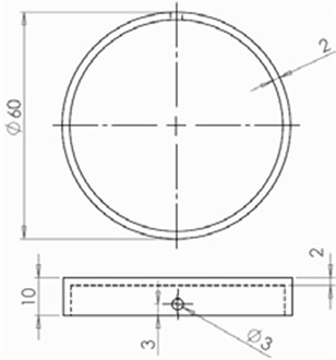
Fig. 14Stack type piezoactuator PSt 150/4/20 VS9
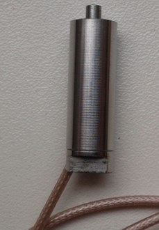
Fig. 15Drawing of vibroactive pad (1 – upper part of aluminum frame; 2 – low frequency stack type piezoactuator; 3 – bottom part of aluminum frame) [59]
![Drawing of vibroactive pad (1 – upper part of aluminum frame; 2 – low frequency stack type piezoactuator; 3 – bottom part of aluminum frame) [59]](https://static-01.extrica.com/articles/15911/15911-img16.jpg)
In previous works by Kaunas University of Technology team and scientists worldwide it was shown that the high frequency vibrations improve the quality of periodical microstructure replicas. The aim of this Master Thesis is to analyze how different process regimes with the help of high frequency vibrations improve the quality.
In the experiment both vibroactive pads (1st and 2nd generation) were used. They excited two forms of vibrations (Fig. 17-20). All other process parameters can be seen in the Table 6.
Fig. 16Manufactured vibroactive pads: a) 1st generation, with piezoelectric ring; b) 2nd generation, with stack type piezoactuator [59]
![Manufactured vibroactive pads: a) 1st generation, with piezoelectric ring; b) 2nd generation, with stack type piezoactuator [59]](https://static-01.extrica.com/articles/15911/15911-img17.jpg)
a)
![Manufactured vibroactive pads: a) 1st generation, with piezoelectric ring; b) 2nd generation, with stack type piezoactuator [59]](https://static-01.extrica.com/articles/15911/15911-img18.jpg)
b)
Fig. 171st vibration form of 1st generation vibroactive pad (f= 5.2 kHz; U= 5 V)
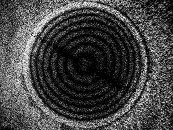
Fig. 182nd vibration mode of 2nd generation vibroactive pad (f= 8.8 kHz; U= 40 V)
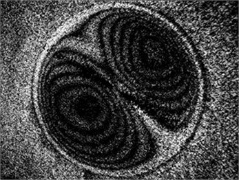
Fig. 191st vibration mode of 2nd generation vibroactive pad (f= 12.910 kHz; U= 3.5676 V)
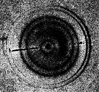
Fig. 202nd vibration mode of 2nd generation vibroactive pad (f= 13.601 kHz; U= 4.4416 V)
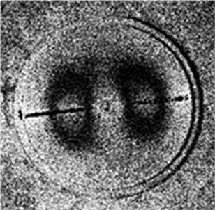
Table 6Periodical microstructure replication process regimes
Vibrations | Pressure | Temperature | Time |
No vibrations 1st form of vibrations (12.910 kHz; 3.5676 V) 2nd form of vibrations (13.601 kHz; 4.4416 V) | 0.1 MPa 0.2 MPa 0.3 MPa 0.4 MPa 0.5 MPa 0.6 MPa | 148°C 152°C | 5 s 10 s 15 s |
All replication process parameters were used for replication of periodical microstructures in random order. 49 periodical microstructure replicas were made with the 1st generation vibroactive pad and 20 – with the 2nd generation vibroactive pad.
9. Conclusions
In the paper investigation techniques, which are necessary for investigation of outcomes of ultrasonic hot embossing process as well for dynamic analysis of vibroactive pad, which is employed during the imprint process are presented with all the specifications and discussed.
During the dynamic analysis of two different vibroactive pads performed with PRISM system was revealed, that first and second vibration modes of first generation vibroactive pad are at following parameters respectively: 5.2 kHz; 5 V and 8.8 kHz; 40 V. Whereas first and second vibration modes of second generation vibroactive pad, based on stack type multilayer actuator are as following: 12.910 kHz; 3.5676 V and 13.601 kHz; 4.4416 V.
References
-
Palmer Ch. Grating Handbook. Newport Corporation, 2014, p. 204.
-
Loewen E. Diffraction Grating Handbook 4th Edition. Richardson Grating Laboratory, 2000, p. 143.
-
Gale M. T. Replication technology for holograms and diffractive optical elements. Journal of Imaging Science and Technology, Vol. 41, 1997, p. 211-220.
-
Janušas G. Formation and investigation of periodical microstructures using coherent radiation. Doctoral dissertation, Technologic Sciences, Mechanical Engineering, Kaunas, 2008, p. 102.
-
GSolver User Guide, http://www.gsolver.com/UserManual.pdf.
-
Narijauskaitė B. Development and study of microrelief formation method. Doctoral dissertation, Kaunas, 2013, p. 7-8, (in Lithuanian).
-
Palevičius A., Janušas G., Ostaševičius V., Bansevičius R. P., Busilas A., Rubliauskas D. Analysis dynamics of piezoelectric optical scanner with periodical microstructure. Active and Passive Smart Structures and Integrated Systems, Vol. 6928, 2008.
-
Zeng Y., Qiab L., Bing Y., Wen M., Zou B., Zheng W., Zhang T., Zou G. Development of microstructure CO sensor based on hierarchically porous ZnO nanosheet thin films. Sensors and Actuators B: Chemical, Vol. 173, 2012, p. 897-902.
-
Zhang T., Liu L., Qi Q., Li S., Lu G. Development of microstructure In/Pd-doped SnO2 sensor for low level CO detection. Sensors and Actuators B: Chemical, Vol. 139, 2009, p. 16-24;
-
Laser Focus World, http://www.laserfocusworld.com/articles/2011/02/hydrogels-used-to.html.
-
Bai W., Spivak D. A. A Double-Imprinted Diffraction-Grating Sensor Based on a Virus-Responsive Super-Aptamer Hydrogel Derived from an Impure Extract. Angewandte Chemie International Edition in English, 2014.
-
Steingrüber R., Ferstl M., Pilz W. Micro-optical element fabricated by electron-beam lithography and dry etching technique using top conductive coatings. Microelectronic Engineering, Vol. 57-58, 2001, p. 285-289.
-
Ahn S. W., Lee K. D., Kim J. S., Kim S. H., Lee S. H., Park J. D., Yoon P. W. Fabrication of subwavelength aluminum wire grating using nanoimprint lithography and reactive ion etching. Microelectronic Engineering, Vol. 78-79, 2005, p. 314-318.
-
Te Kolste R. D., Welch W. H., Foldman M. R. Injection moulding for diffractive optics. Proceedings of SPIE, 1995, p. 129-131.
-
Leech P. W., Lee R. A., Brett A. Sexton and Fiona Smith Hot embossing of micrographic elements in polypropylene. Microelectronic Engineering, Vol. 84, 2007, p. 109-113.
-
Lebib A., Chen Y., Bourneix J., Carcenac F., Cambril E., Couraud L., Launois H. Nanoimprint lithography for large area pattern replication. Microelectronic Engineering, Vol. 46, 1999, p. 4129-4133.
-
Singh S. Diffraction gratings: aberrations and applications. Optics and Laser Technology, Vol. 31, 1999, p. 195-218.
-
Worgull M., Hetu J. F., Kabanemi K. K., Heckele M. Modeling and optimization of the hot embossing process for micro- and nanocomponent fabrication. Microsystem Technologies, Vol. 12, 2006, p. 947-952.
-
Nadir A. Roll to Roll UV Embossing Technology. The Holography Times, 2010, p. 12-14.
-
Piotter V., Hanemann T., Ruprecht R., Haußelt J. Injection molding and related techniques for fabrication of microstructures. Microsystems Technologies, Vol. 3, 1997, p. 129-133.
-
Su Y., Shah J., Liwei L. Implementation and analysis of polymer microstructure replication by micro injection molding. Journal of Micromechanics and Microengineering, Vol. 14, 2004, p. 415-422.
-
Qin D., Xia Y., Rogers J., Jackman R., Zhao X., Whitesides G. Microfabrication, microstructures and microsystems. Topics in Current Chemistry, Vol. 194, 1998.
-
Li J. M., Liu C., Peng J. Effect of hot embossing process parameters on polymer flow and microchannel accuracy produced without vaccum. Journal of Materials Processing Technology, Vol. 207, 2008, p. 163-171.
-
Heckele M., Backer W., Müller K. D. Hot embossing – the molding technique for plastic microstructures. Microsystems Technologies, Vol. 4, 1998, p. 122-124.
-
Juang Y., James Lee L., Koelling K. Hot embossing in microfabrication. Part I: Experimental. Polymer Engineering and Science, Vol. 42, 2002, p. 539-550.
-
He Y., Fu J., Chen Z. Research on optimization of the hot embossing process. Journal of Micromechanics and Microengineering, Vol. 17, 2007.
-
Heyderman L. J., Schift H., David C., Gobrecht J., Schweizer T. Flow behaviour of thin polymer films used for hot embossing lithography. Microelectronic Engineering, Vol. 54, 2000, p. 229-245.
-
Heyderman L. J., Schift H., Auf der Maur M., Gobrecht J. Pattern formation in hot embossing of thin polymer films. Nanotechnology, Vol. 12, 2001.
-
Narijauskaitė B., Gaidys R., Palevičius A., Janušas G. Simulation of hot imprint process of periodic microstructure using elasto-plastic material model. Journal of Vibroengineering, Vol. 13, Issue 2, 2011.
-
Narijauskaitė B., Palevičius A., Narmontas P., Ragulskis M., Janušas G. High-frequency excitation for thermal imprint of microstructures into a polymer. Experimental Techniques, Vol. 10, 2012.
-
Šakalys R., Janušas G., Palevičius A. Quality analysis of periodical microstructures, created by using high frequency vibration excitation. International Electronic Conference on Sensors and Applications, 2014.
-
Bakšys B., Puodžiūnienė N. Alignment of parts in automatic assembly using vibrations. Assembly Automation, Vol. 27, 2007, p. 38-43.
-
Yule A. J., Al-Suleimani Y. On droplet formation from capillary waves on a vibrating surface. Mathematical, Physical and Engineering Sciences, Vol. 456, 2000, p. 1069-1085.
-
Dong L., Chaudhury A., Chaudhury M. K. Lateral vibration of a water drop and its motion on a vibrating surface. The European Physical Journal, Vol. 21, 2006, p. 231-242.
-
Khuntontong P., Blaser T., Schomburg W. K. Ultrasonic micro hot embossing of polymer exemplified by a micro thermal flow sensor. Proceedings of Smart System Integration, 2008, p. 327-334.
-
Khuntontong P. Fabrication of Polymer Micro Devices by Ultrasonic Hot Embossing. Doctoral dissertation, Technologic Sciences, Mechanical Engineering, Thailand, 2008, p. 84.
-
Midlin R. D. High frequency vibrations of piezoelectric crystal plates. International Journal of Solids and Structures, Vol. 8, 1972, p. 895-906.
-
Narijauskaitė B., Palevičius A., Janušas G., Šakalys R. Numerical investigation of dynamical properties of vibroactive pad during hot imprint process. Journal of Vibroengineering, Vol. 15, Issue 4, 2013, p. 1983.
-
Šakalys R., Palevičius A., Janušas G. Vibroactive pad improvement using stack type piezoactuator. Vibroengineering Procedia, Vol. 2, 2013, p. 103-112.
-
Šakalys R., Janušas G., Palevičius A. Vibroactive pad for replication of microstructure and its experimental analysis. Proceedings of the 19th International Conference Mechanika, 2014, p. 225-227.
-
Narijauskaitė B. Microrelief formation by mechanical imprint method. Doctoral dissertation, Technologic Sciences, Mechanical Engineering, Kaunas, 2012, p. 112.
-
Loewen E. G., Popov E. Diffraction Gratings and Applications, Optical Engineering Series. Marcel Dekker, New York – Basel, 1997, p. 601.
-
Xie H., Shang H., Dai F., Li B., Xing Y. Phase shifting SEM moiré method. Optics and Laser Technology, Vol. 36, 2004, p. 291-297.
-
Vass C., Osvay K., Csete M., Hopp B. Fabrication of 550 nm grating in fused silica by laser induced backside wet etching technique. Applied Surface Science, Vol. 253, 2007, p. 8059-8063.
-
Sai H., Yugami H., Akiyama Y., Kanamori Y., Hane K. Spectral control of thermal emission by periodic microstructured surfaces in near-infrared region. Optics InfoBase, Vol. 18, 2001, p. 1471-1476.
-
Medway Optics LTD, http://www.medwayoptics.com/product4.htm.
-
Antos R., Ohlidal I., Mistrik J., Murakami K., Yamaguchi T., Pistora J., Horie M., Visnovsky S. Spectroscopic ellipsometry on lamellar gratings. Applied Surface Science, Vol. 244, 2005, p. 225-229.
-
Orbons S. M., Dijk L., Bozkurt M., Johnston P. N., Reichart P., Jamieson D. N. Focused ion beam machined nanostructures depth profiled by macrochannelling ion beam analysis. Nuclear Instruments and Methods in Physics Research B, Vol. 249, 2006, p. 747-751.
-
Narijauskaitė B., Palevičius A., Gaidys R., Janušas G. Polycarbonate as elasto-plastic material model for simulation of hot imprint process of microstructure. 25th International Symposium on Polymer Analysis and Characterization, 2012, p. 23.
-
Oštaševičius V. Applicability of holographic technique for analysis of non-linear dynamics of MEMS switch. Proceesing of SPIE: Smart Structures and Materials: Smart Electronics, MEMS, BioMEMS, and Nanotechnology, Vol. 5763, 2005, p. 405-413.
-
Palevičius A. Digital holography for analysis of mechatronic systems. Proceedings of the 7th International Conference Vibroengineering, 2008, p. 78-82.
-
Kaunas University of Technology, http://ktu.edu/im/turinys/holografine-sistema-prism.
-
Rimašauskienė R. Investigation of dynamic of smart valve using holographic PRISM system. Journal of Vibroengineering, Vol. 12, 2010, p. 443-452.
-
Popov E. Gratings: Theory and Numeric Applications. Institut Fresnel, 2012, p. 23.
-
Lee W., Levent Degertekin F. Rigorous Coupled-wave analysis of multilayered grating structures. Journal of Lightwave Technology, Vol. 22, 2004, p. 2359.
-
Liu S., Ma Y., Chen X., Zhang C. Estimation of the convergence order of rigorous coupled-wave analysis for binary gratings in optical critical dimension metrology. Optical Engineering, Vol. 51, 2012, p. 7.
-
Chateau N., Hugonin J. Algorithm for the rigorous coupled-wave analysis of grating diffraction. Journal of the Optical Society of America A, Vol. 11, 1994, p. 1321-1331.
-
Goray L. I. Modified integral method for weak convergence problems of light scattering on relief grating. Diffractive and Holographic Technologies for Integrated Photonic Systems, Vol. 4291, 2001, p. 1-12.
-
Šakalys R., Janušas G., Palevičius A. Vibroactive pad for replication of microstructure and its experimental analysis. Proceedings of 19th International Conference Mechanika, Kaunas, p. 3.
About this article

This research was funded by a Grant (No. MIP-026/2014) from the Research Council of Lithuania.
