Abstract
This paper covers the investigations of periodical microstructures formed in novel PVDF-based thin films. The design concept consists of a tunable periodical microstructure embossed onto thin film. The tuned grating element was fabricated by hot-embossing method. Research results show that piezoelectric properties of thin film gives significant changes of periodical microstructure parameters (grating depth, width) and its optical response (diffraction efficiencies) when voltage is applied. Thus, the ability to tune a periodical grating microstructure and implement it as a modulating optical element of a lightsource holds great promise in design of novel optical microsystem devices for medical or spectroscopy applications.
1. Introduction
The challenge to design structures, which have great technical and scientific values, has attracted the attention of scientists and technicians. Microdevices based on optical method benefit from the fact that this method is not affected by electromagnetic interference. This is a critical limitation for highly integrated devices. As for optical sensing devices, usage of periodical microstructures is great of value because of its remote control and friction-free characteristics.
Recent researches are related to design of digital and analog tunable gratings for optical microelectromechanical devices. Tunable gratings as digital include polychromators [1, 2], grating light valves [3], liquid-crystal phased arrays [4], gratings driven by thin-film piezoelectric microelectromechanical (MEMS) actuators, etc. Analog include thermal actuation [5], acoustic [6], electrostatic actuation [7] based mechanism gratings, etc. Today, one of main researcher’s tasks is to achieve high tunability in the diffracted angle with a high resolution of the order when designing accurate and sensitive microdevices.
Devices fabricated from active materials and characterized by sensing and actuating functions are designed to detect and react to changes in their operating environment, like pressure, bending forces or impact. Among piezoelectric films, the majority of MEMS sensing and actuating devices comprises of Lead Zirconium Titanate (PZT), Polyvinylidene fluoride (PVDF) and Barium Titanate (BaTiO3). A thin film of piezoelectric material with metal electrodes on the opposite sites, vibrates when alternating voltage of a matching frequency is applied. This unique property provides an opportunity for a real time and direct observations of affinity interactions [8]. For a tunable grating [9, 10], the oscillation frequency is determined by resonator, and measured with a counter. Such signals (quality factor, impedance of the resonator) on viscoelastic effects in solution can be obtained. If constant potential is applied on one side of the resonator versus reference electrode, electrochemical reactions can be followed together with the mass changes. Combination of thin piezoelectric film and periodical microstructure in one single element can lead to more sensitive and higher response speed of the overall sensing device [11, 12].
The ability to tune a periodical grating microstructure and implement it as a modulating optical element of a lightsource holds great promise. This paper covers investigation of thin film PVDF-PMMA-BaTiO3 with periodical microstructure. Results showed that designed tunable optical element changes its grating parameters (grating depth, width) and optical response (diffraction efficiencies) under certain applied bias.
2. Experimental details
2.1. Materials, synthesis and formation
Piezoelectric materials distinguish themselves with a high bandwidth, high frequency, low power requirements, fast response and high generative forces. Polyvinylidene fluoride (PVDF) proved its usefulness in sensing and actuating applications because changes in the surroundings don’t influence PVDF piezoelectric properties and it still can maintain its inherent damping capacity and not loose piezoelectric response. Barium Titanate has markible properties among inorganic compounds like photorefractive effect, good mechanical and chemical stability, electrical properties, and easiness in its preparation. Thus, blending of different polymers is one of techniques used to improve some physical properties of homopolymers. PVDF and PMMA exhibit a lower critical solution temperature (~300 C°) and are completely miscible in the melt [13]. Combining properties of both piezoelectric materials, novel material PVDF-PMMA-BaTiO3 with specific properties was created. Poly (methyl methacrylate) PMMA here is used because of the direct influence to PVDF-based thin film properties, i.e. to force PVDF to crystallize into the piezoelectric phase.
Previous researches showed that piezoelectric polymer systems may be achieved using inexpensive method when blending PVDF with other polymers. The piezoelectricity of PVDF blends is strongly affected on the nature of blending polymers and by the final PVDF crystal structure [14]. It also depends on the PVDF molecular and supermolecular structure as well as on electrical and mechanical properties of the crystalline and amorphous regions [15]. This method allows to control the crystalline phase of PVDF, too [14, 15]. Thus, because of substitution of PMMA the piezoelectric elementary cells have a uniform orientation after thin film formation, thus no poling is needed.
Table 1Materials and synthesis of PVDF-based thin film
Materials | Preparation of blend |
PVDF-PMMA-BaTiO3 | 5 % PVDF (average 34000) and barium titanium oxide BaTiO3 were taken in suitable and definite compositional ratios and mixed with appropriate amount of 5 % PMMA (average 15000) |
PVDF-based thin film was deposited on 50 µm thickness copper foil substrate. Simple and inexpensive method was used for thin film formation – a spin-coating technology by means of centrifuge “Dynapert Precima”. A hot-embossing technology was used to fabricate periodical microstructure onto PVDF-PMMA-BaTiO3 thin film with high accuracy. For high-throughput replication technology a 4 micron and 700 nm depth master grating was used.
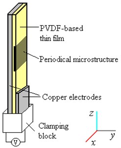
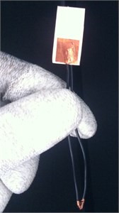
Fig. 1a) Design schematic of a tunable PVDF-based optical element; gratings, defined on top of thin film, are tuned progressively along with the film, b) Prototype of the element
a)
b)
2.2. Concept and design
A designed optical element with piezoelectric properties is one-step ahead by applying tunable periodical microstructures for biological imaging in microsystems. To achieve this, first a thin PVDF-based film was coated on a copper foil. Periodical microstructure is formed parallel to the short edge. On top of one thin film edge, a copper electrode is formed. Simple in design this optical element is shown in Fig. 1.
The ability to tune a periodical grating (Fig. 1) and implement it as a modulating optical element of a lightsource, holds great promise in design of novel optical microsystem devices for biomedical or spectroscopy applications.
2.3. Analytical equipment
For the measurements and analysis of surface morphology and elastic properties of thin films – Atomic Force Microscopy (AFM NT-206) was applied.
For experimental setup of applying external voltage a power supply and a multimeter were used. The top and bottom electrodes of the element were attached to aluminum tape to facilitate connections to the supply when applying defined bias. The junctions between the tape and electrodes were coated by silver paint. The complete element was mounted into AFM and diffractometer for further investigations.
For measurements of diffraction efficiency in all peaks for different incident angles, a laser diffractometer was used. It consists of He-Ne laser source, set of mirrors to direct a beam, photodiode and a tester, to record the measurement data. Red He-Ne laser of a wavelength 632.8 nm incident to grating was used for measurements.
3. Results and discussions
Good mechanical and optical properties, sensitivity, morphology, response speed and strong power are foreseen for functional elements in microdevices. Atomic Force Microscopy technique allows evaluations and meticulous observations of the various characteristics including textural and morphological of PVDF-based thin film. Surface morphology of PVDF-PMMA-BaTiO3 thin film was evaluated with AFM NT-206. Results showed that fabricated thin film has rather smooth surface of only 38.2 nm roughness. There are seen small islands and irregularities on the surface of thin film with average depth of 169 nm and width of 337 nm. Main results are given in Table 2.
Table 2Basic morphological properties of PVDF-based thin film
Parameters | Values | AFM results |
, nm | 31.2 | 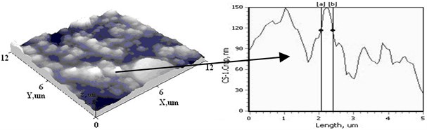 |
, nm | 38.2 | |
, nm | –0.09 | |
Max. height , nm | 169 | |
Grain diameter, nm | 337 | |
Adhesion force, nN | 1903 | 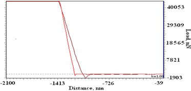 |
Maximum load, nN | 40053 |
Previous researches [16, 17] showed the influence of PMMA for surface, mechanical and optical properties of various piezoelectric thin films. Here, PVDF-based thin film has adhesion of about 1903 nN describing elasticity of the element (Load-Distance curve in Table 2). It is one of the basic mechanisms of friction and also influences the deformation of thin films when gratings are imprinted. So, the final step is formation of a regular shape grating onto thin film. Its parameters are dependent on properties of thin film surface. Thus, using a 4 micron master grating a well-defined periodical microstructure was formed. Results are presented in Table 3.
Table 3Main properties of tunable PVDF-based optical element
Parameters | Values | AFM results |
Average depth, μm | 0.78 | 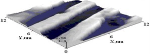 |
Average width, μm | 3.4 | |
, μm | 0.3 |
For measurements of diffraction efficiency in all peaks of different incident angles a laser diffractometer was used. Distribution of diffraction efficiency was observed in 0, ±1 ±2 and ±3 order maxima. Characteristics of efficiencies were registered and given in Fig. 2.
Fig. 2Diffraction efficiencies of tunable optical element
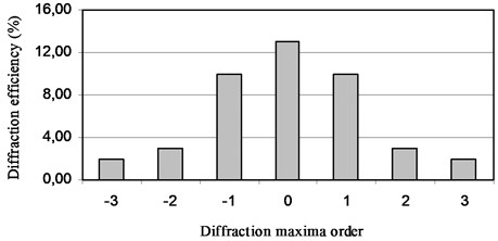
As diffraction efficiency measurements shows that a periodical microstructure imprinted on PVDF-PMMA-BaTiO3 thin film concentrated its diffracted energy it’s zero order about 13 % and in its first orders of its maxima 10 %. About 3 % of diffracted energy were concentrated in its second order of maxima. Thus, diffraction efficiencies in 0 and ±1 orders of its maximum are of most importance and results are dependent on imprinted grating, i.e. its parameters and form similar to master grating.
Fig. 3Changes of average grating depth and width (observed by AFM) under external bias
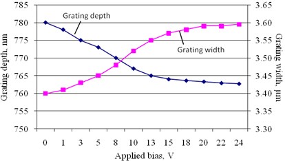
Designed PVDF-based optical element is a voltage driven thin film able to change the geometry (or, so called relief) of a periodical microstructure. To prove the relevance of designed tunable optical element, measurements of PVDF-PMMA-BaTiO3 periodical microstructure response to applied voltage were performed. Using AFM, the differences of microstructure relief to applied voltage were evaluated and given in Fig. 3.
Obtained results showed, that applying voltage from 0 to 13 V there are observed significant changes in microstructure depth and width. Thus, the average depth decreases by approximately 14 nm and the average width of the grating increases by ~0.15 µm. Applied voltage from 13 to 24 V gives very small changes in periodical microstructure parameters, i.e. the average depth changes by ~1.3 nm and average width by ~0.025 µm. Moreover, the element provides a new way of lightsource modulation under applied voltage. So, for the evaluation of optical response of a periodical microstructure with changed parameters, a laser diffractometer was used. Diffraction efficiencies were measured in 0, ±1 and ±2 orders of its maxima using laser light of wavelength 632.8 nm incident to grating. Results are given in Fig. 4.
Fig. 4Dependence of diffraction efficiency on applied voltage
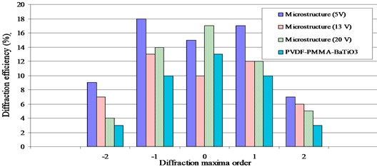
Results in Fig. 4 give the response of a working element. It shows that designed tunable optical element changes its grating parameters together with optical response under a certain applied bias. Thus, diffraction efficiencies of PVDF-PMMA-BaTiO3 periodical microstructure, when voltage of 5 V and 13 V was applied, have changed in its zero order by 5 %, in its first orders by 4 %, respectively. When 20 V voltage was applied, most of the diffraction efficiencies is concentrated in its zero and first orders.
An element also possesses a unique ability to be configured into an infinite number of shapes and sizes, for extreme application versatility. Property of piezoelectricity in optical element was introduced in order to improve the usability as a new technology for sensing or biosensing systems in various applications.
The suitability of designed novel PVDF-based element is interest for cell force sensing applications due to its linear coupling of force and electrical charge [17, 18]. Also, it may be used for power harvesting in biomedical implants due to element ability to generate electrical charges without any contact with the environment outside of the host. In general it would be possible to harvest energy either from voluntary movements such as walking or from continuous movements such as heartbeat, pulse, breathing, etc.
4. Conclusions
PMMA plays an important role, leading to imprint of well–defined periodical microstructures. Formed symmetrical grating in PVDF-PMMA-BaTiO3 influence sensitivity of a tunable optical element, i.e. the results of diffraction efficiencies in zero and first orders of its maxima were concentrated with only small differences from 2 % to 13 %.
Results of tunable PVDF-based optical element with piezoelectric properties proved the relevance of voltage-driven grating which changes its geometrical parameters when voltage is applied, i.e. the average grating depth decreases by approximately 14 nm and the average width of the grating increases by ~0.15 µm.
The ability to tune a periodical microstructure and implement it as a modulating optical element of a lightsource holds great promise in design of novel optical microsystem devices for biomedical or spectroscopy applications.
References
-
Jinto T., Ajai K., Vishnu C., Kaushal P., Ranjeet S. Design and development of five-channel interference filter polychromator for SST-1 Thomson scattering system. Fusion Engineering and Design, Vol. 87, Issue 2, 2012, p. 134-140.
-
Hocker G. B., Youngner D., Deutsch E., Volpicelli A., Senturia S., Butler M., Sinclair M., Plowman T., Ricco A. J. The polychromator: a programmable MEMS diffraction grating for synthetic spectra. Technical Digest of the Solid-State Sensors and Actuators Workshop, 2000, p. 89-92.
-
Rudra S., Roels J., Bryce G., Haspeslagh L., Witvrouw A., Thourhout D. SiGe based grating light valves: A leap towards monolithic integration of MOEMS. Microelectronic Engineering, Vol. 87, Issue 5-8, 2010, p. 1195-1197.
-
Wang X., Tan Q., Huang Z., Tang Z. Liquid crystal optical phased array device with a fine steering precision of a few micro-radians. Optics Communications, Vol. 313, 2014, p. 360-364.
-
Riahi M. Design and fabrication of a Fourier transform spectrometer by means of thermally actuated tunable grating. International Journal for Light and Electron Optics, Vol. 123, Issue 8, 2012, p. 684-687.
-
Cox T. J., D’Antonio P. Acoustic phase gratings for reduced specular reflection. Applied Acoustics, Vol. 60, Issue 2, 2000, p. 167-186.
-
Sene D. E., Grantham J. W., Bright V. M., Comtois J. H. Development and characterization of micro-mechanical gratings for optical modulation. Proceedings of the 9th Annual International IEEE Micro Electro Mechanical Systems Workshop, 1996, p. 222-227.
-
Pohanka M., Skládal P., Pavliš O. A label free piezoelectric immunosensor for rapid assay of Escherichia coli. Journal of Immunoassay and Immunochemistry, Vol. 29, 2008, p. 70-79.
-
Liu T. K., et al. Fabrication of tunable grating with silver nanoparticles. Proccedings of SPIE, 2009, p. 7390.
-
Wong C. H., Yongbae J., Barbastathis G., Sang-Gook K. Analog piezoelectric-driven tunable gratings with nanometer resolution. Journal of Microelectromechanical Systems, Vol. 13, Issue 6, 2004.
-
Wong C. H., Yongbae J., Barbastathis G., Sang-Gook K. Analog tunable gratings driven by thin-film piezoelectric microelectromechanical actuators. Applied Optics, Vol. 42, Issue 4, 2003, p. 621-626.
-
Jeon J., Kang S., Lee S., Oh I. Novel biomimetic actuator based on SPEEK and PVDF. Sensors and Actuators B: Chemical, Vol. 143, Issue 1, 4, 2009, p. 357-364.
-
Elashmawi I. S., Hakeem N. A. Effect of PMMA addition on characterization and morphology of PVDF. Polymer Engineering and Science, Vol. 48, Issue 5, 2008, p. 895-901.
-
Abbas R. R., Rammo N. N., Al-Ajaj E. A. Structure and piezoelectricity in blends of PVDF films PVDF. Journal of Kerbala University, Vol. 6, Issue 4, 2008, p. 201-208.
-
Hahn B. R., Wendorff J. H. Piezo- and Pyroelectricity of Poly (vinylidene fluoride) / Poly (methyl methacrylate). Polymer, Vol. 26, 1985, p. 1611.
-
Ponelytė S., Guobienė A., Puišo J., Palevičius A., Prosyčevas I. Intelligent piezoelectric polymers PVDF-PZT for biosensing applications. Journal of Vibroengineering, Vol. 14, Issue 1, 2012, p. 236-243.
-
Ponelytė S. Creation, Investigation and Application of Novel Nanocomposite Thin Films with Periodical Microstructure. Doctoral dissertation, Kaunas University of Technology, Kaunas, 2013, p. 123.
-
Wang X. Piezoelectric nanogenerators-harvesting ambient mechanical energy at the nanometer scale. Nano Energy, Vol. 1, Issue 1, 2012, p. 13-24.
About this article

The part of this research work was funded by EU Structural Funds Project “Microsensors, Microactuators and Controllers for Mechatronics Systems (Go-Smart)” (Nr. VP1-3.1-ŠMM-08-K-01-015).
The part of this research work was funded by a Grant (No. MIP-026/2014) from the Research Council of Lithuania.
