Abstract
In this paper, the types of penetrating collision overload signals are analyzed, and a detection device for simulating the signal of the penetration process is designed in combination with engineering practice. The device uses asimulated signal generation circuit to simulate the overload signal of the projectile actually hitting the target during the penetration process. The Pspice simulation software is used to simulate the voltage overload of the simulated overload signal, and the feasibility and stability of the signal generation are verified by the prototype test. The simulation signal proposed by the design scheme can be used to simulate the penetration overload signals for different initial speeds and different targets, and it has certain guiding significance for the pre-design simulation test of engineering projects.
1. Introduction
In engineering practice, whether it is a car collision or a projectile penetration, it will produce high impact and high overload during its action. In many cases, an acceleration sensor is often used to collect an overload signal. Due to the harshness and high cost of dynamic test conditions, it is necessary to test the product before the test to improve the reliability and safety of the product.
In the test, the signal generating device designed in this paper is used to simulate the actual sensor's action before the test, and the test data is more reasonable and reliable. Signal generators can be used for the simulation of sensor signals, but have the following disadvantages: first, in production practice, in the face of high-volume production test requirements, the use of signal generators will increase production costs; second, signal generators can only The generation of periodic waveform signals, the inability to achieve accurate delay, variable-cycle signals, and the simultaneous generation of multiple forms of waveforms, so that it can’t accurately simulate the penetration process signal, thus greatly reducing the reliability of the test. Therefore, the use of electronic circuit technology to simulate the generation of overload signals has arisen. The use of circuits to simulate overload signals can greatly reduce production costs and facilitate high-volume, large-scale production [1].
2. Signal type and generating principle
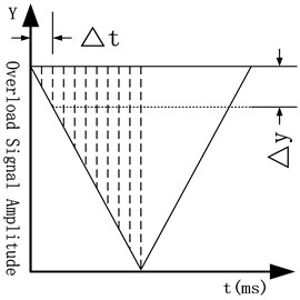
In the process of projectile penetration, the penetration overload signal is similar to the triangular wave. The bottom edge of the triangle wave is the pulse width of the overload signal, and the amplitude is the overload value [2]. Therefore, the signals to be simulated in this paper are upper and lower triangular waves whose amplitude and pulse width can be adjusted, which are used to simulate multi-layer target penetration, different target thickness penetration, and internal overload.
The acceleration sensor collects an overload signal and outputs the overload signal as a voltage. Therefore, it is necessary to estimate the approximate amplitude and pulse width of the overload signal, and then use the electronic circuit combined with the software to simulate different penetration overload conditions.
3. Overload signal generation scheme and simulation
The signal source in the simulated overload signal generation circuit is generated by the MCU. After being processed by the peripheral circuit such as the filter circuit and the voltage follower circuit, the required simulated overload signal is output, and the signal transmission block diagram is shown in Fig. 1.
Fig. 1Signal transmission block diagram

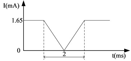
The front-end signal of this paper is generated by the internal 12-bit current digital-to-analog converter (IDAC) of the MCU. The maximum current of the IDAC setting output is 2 mA. For example, the simulated overload with an output pulse width of 2 ms and overload amplitude of 1.65 V is taken as an example. The resulting signal waveform is shown in Fig. 2.
Fig. 2Front end current signal waveform
The previous stage current signal is converted to an intermediate straight voltage signal with maximum amplitude of 1.65 V and minimum amplitude of 0 V through the current/voltage conversion module. Since the test target has a reflow impact on the simulated overload signal during the test, a voltage follower is added after the intermediate voltage signal is output to avoid the influence of the external circuit on the stability of the simulated overload signal. The resulting intermediate DC voltage signal is subjected to voltage follow-up processing by means of Pspice software.
Fig. 3Voltage follower schematic
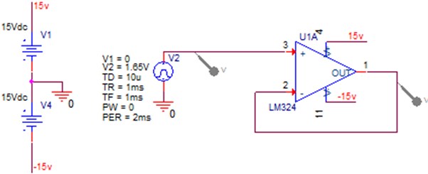
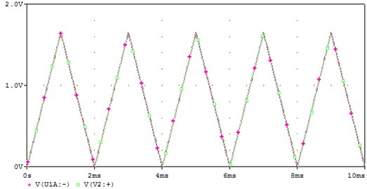
The voltage following principle is shown in Fig. 3. The LM324 chip has low output impedance and large input impedance, which improves the stability and anti-interference ability of the intermediate signal. The LM324 chip is powered by ±15 V, and the current signal generated by the MCU passes through the same input of the 820 Ω input voltage follower. The simulation waveform is shown in Fig. 4.
The input waveform is a simulated overload signal with a pulse width of 2 ms and amplitude of 1.65 V. It can be seen from the simulated waveform diagram that the input and output waveforms are basically coincident, and the LM324 voltage follower has obvious voltage follow-up effect on the simulated overload signal, and the signal has no distorted phenomenon [3].
Fig. 4Voltage follow simulation waveform
4. Hardware design
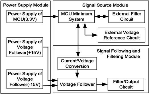
According to the design requirements and the Pspice simulation model, the circuit is fabricated and the experiment is verified. The circuit function and module block diagram are shown in Fig. 5. The simulated overload generating circuit includes three modules: a power module, a signal source generating module, and a signal following filtering module. Among them, the power module includes: MCU power supply (3.3 V) and amplifier chip power supply (±15 V) three major parts [4]. The signal source generation module includes: an MCU minimum system, a filter circuit, and an external voltage reference circuit. The signal following filter module comprises: a current/voltage conversion circuit, a voltage follower, and a filter/output circuit for converting the front end signal into a voltage signal [1].
Fig. 5Circuit function and module block diagram
5. Software design
After estimating the amplitude and pulse width of the approximate overload signal, the signal is divided into several equal points according to the pulse width time direction [5]. As shown in Fig. 6, using the same slope formula, the following formula can be obtained:
According to the relationship table between the output current and the IDAn data word in the MCU data sheet, the IDAn data word required for the simulated overload signal can be derived:
where: – overload signal amplitude, – overload signal pulse width, – the voltage required by the microcontroller, – the data word required by IDAC.
Fig. 6Simulated signal diagram
6. Results and analysis
According to the hardware circuit design, production circuit (shown in Fig. 7), and test (shown in Fig. 8).
Fig. 7Analog overload signal generation circuit
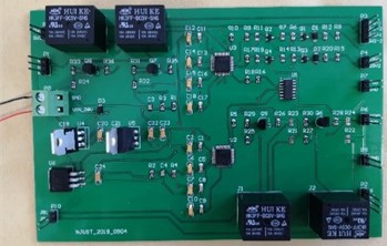
Fig. 8Signal waveform acquisition
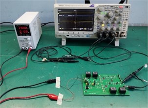
Fig. 9Overload in the crucible
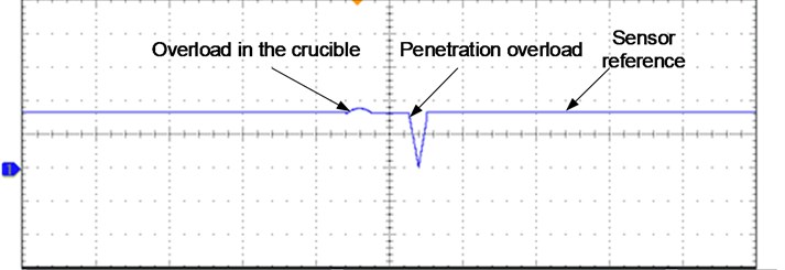
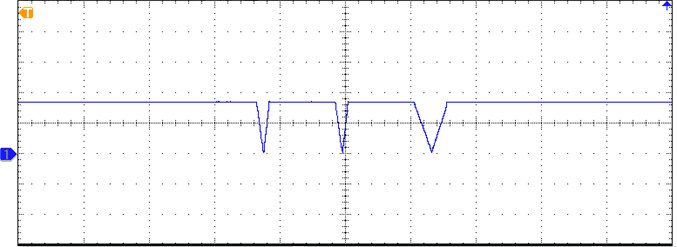
Fig. 10Multi-layer and different target thickness simulated overload signals
7. Conclusions
1) The use of electronic circuit technology combined with software programming to simulate the penetration overload signal is easy to implement in principle, low cost, suitable for industrial mass production and laboratory testing [1].
2) After testing and simulation verification, the simulated overload signal can effectively guarantee the stability and anti-interference ability of the simulated signal under the action of the voltage follower [6].
3) This scheme can simulate the penetration overload signal in various situations, such as: overload in the crucible (shown in Fig. 9), multi-layer target penetration, and different target thickness penetration (shown in Fig. 10).
References
-
Hu Defu, Li Changsheng, Miao Donghui, et al. Study of the alternative scheme for pulse signal of velocity measurement. Advanced Information Management, Communicates, Electronic and Automation Control Conference, 2018, p. 1194-1198.
-
ChienHung-Chun A current-/voltage-controlled four-slope operation square-/triangular-wave generator and a dual-mode pulse width modulation signal generator employing current – feedback operational amplifiers. Mechatronics, Vol. 22, Issue 5, 2012, p. 544-551.
-
Almashary B., Alhokail H. Current-mode triangular wave generator using CCIIs. Microelectronics Journal, Vol. 31, Issue 4, 2000, p. 239-243.
-
Chen Xiao, Chen Jianxiang Design of an arbitrary waveform signal generator. Procedia Engineering, Vol. 15, 2011, p. 2500-2504.
-
Al-Shahrani M. T. A. New CFOA-based triangular/square wave generator. International Journal of Electronics, Vol. 84, Issue 6, 1998, https://doi.org/10.1080/002072198134427.
-
Tietze D. I. U., Schenk D. I. C., Gamm D. I. E. Signal Generators. Springer Berlin Heidelberg, 2008.
About this article

This work was supported in part by the National Natural Science Foundation of China (Grant No. 61403201), in part by the Advanced Research Project of the 13th Five-Year Plan (Grant No. 41419050104), in part by the Six Talent Peak Projects (KTHY-019), and in part by the National Key Laboratory Foundation (Grant No. 6142601180101).
