Abstract
A numerical model based on the spectral finite element method (SFEM) is proposed to predict the electromechanical impedance (EMI) spectra of the PZT transducer bonded beam. Fast and accurate simulation of the impedance signals from the PZT wafer can be achieved by SFEM. The proposed model includes the PZT wafer (actuator/sensor), beam structure and the coupled interaction between PZT wafer/beam structure, which predicts the frequency response function, the impedance response under damage and temperature variation effects. Numerical simulation algorithms are validated with both finite element analysis and experiments. The results show that the proposed model has capability of capturing the effect of damage and temperature effects on PZT transducer impedance with great accuracy, the existence of damage can be detected by evaluating the electromechanical impedance signals.
1. Introduction
Structural health monitoring (SHM) techniques with regard to piezoelectric materials have been developed to assess the safety and integrity of in-situ structures, such as wave propagation technique [1], electromechanical impedance [2]. When PZT wafers are adopted for damage detection in a plate-like structure, both transient and steady state dynamic responses can be easily generated and measured through the EM interaction between the PZT wafers and the structure. With a transient input excitation, guide ultrasound waves were generated in a plate-like structure. However, the traveling guide ultrasound waves may become standing waves which producing normal vibration modes with a steady state excitation, while the response signals can be reflected by the electromechanical impedance of the PZT wafers. Due to the two-way electromechanical coupling of the PZT wafers, the piezoelectric impedance is directly related to the mechanical impedance of the host structure. EMI technique is considered to be one of the most promising approaches of these piezoelectric SHM techniques due to its high sensitivity to local incipient damage and low-cost [3].
The application of EMI technique to structure health monitoring has its theoretical development first proposed by Liang et al. [4], and several studies have been subsequently developed [5-8]. Giurgiutiu [7] modeled interaction between beam and plate with PWAS, in this model, the insertion of a coupled moment and force on structure (beam/plate) implied to model effect of PWAS actuator. Bhalla and Soh [8] studied two-dimensional interaction of PWAS with structure based on mechanical impedance to determine electrical impedance of PWAS. However, analytical models are often limited in actual application because they are only applicable to simple structures such as beams, plates and shells. Yang et al. [9, 10] presents finite element simulations on the interaction between a piezo-impedance transducer and a structure, and studied the effects of the PZT bonding thickness on the electrical impedance signature. Seyed et al. [11] developed a FEM of a hollow cylinder to study the influence of different damage types and damage location on EMI spectrum. However, the size of each element in FEM should be sufficiently small, especially in a high frequency range, which can increase the computation time and cost significantly. This is necessary for the inertia effect of a structure can be properly evaluated only when the element size is 10-20 times smaller than the wavelength or the modal length of interest [12]. Doyle established the spectral element method (SEM) to study the wave propagation in structures [13]. The SEM is used for modeling a Timoshenko beam in SHM in combination with electric circuit analysis has been studied by Peairs et al. [14]. Based on the SEM, Wang [15] develop a model that can identify both the location and the severity of the damage. A SEM is developed to represent the dynamic response of a coupled piezoelectric wafer and beam system in which either a single or collocated piezoelectric wafers are bonded to a base beam by Park et al. [16]. The SEM uses the frequency dependent shape functions in contrast to the constant polynomial shape functions employed by FEM to construct the element mass and stiffness matrices. Thus it provides accurate dynamic characteristics of a structure and gains very accurate solutions at a high frequency [17]. Although EMI technique shows the characteristics of high sensitivity to incipient damage of host structure, practical problems have hindered the efficient and reliable application of EMI to real-world structures. The current limiting factor of this SHM strategy is the difficulty in differentiating changes due to damage and those caused by changing environmental conditions. Sun et al. [18] used a temperature compensation method based on cross-correlation to correct the horizontal shift in the impedance signature. Park et al. [19] proposed an impedance-based health monitoring technique under a temperature varying environment considering the root mean square deviations of the measured signatures after introducing proper shifts in the horizontal and vertical directions. Bhalla et al. [20] also investigated the influence of the temperature on the impedance signatures. Therefore, it is important to develop the numerical model of a coupled piezoelectric wafer and beam structure to make damage assessment robust for in situ applications and improve monitoring accuracy of the EMI technique.
In this paper, a SFEM is developed to represent the dynamic response of a coupled piezoelectric wafer and beam structure to predict the impedance response under damaged beam and changing temperature. Then the effects of notch damage and temperature on electromechanical signal of the PZT wafer are analyzed by experiments and proposed model.
2. The governing equations
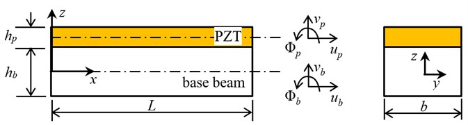
A SFEM was implemented in reference [17], and a one-dimensional spectral model was developed to simulate the dynamic behavior of a beams bonded with PZT wafer. Consider the straight smart beam element with length and width , as shown in Fig. 1. The coupled beam consists of two layers: the PWAS layer of thickness and the base beam of thickness . Assume the beam takes the uniaxial bending vibration in the (, )-plane. The governing equations of the coupled beam will be derived based on the Hamilton’s principle.
Fig. 1Geometry of the elastic-piezoelectric coupled beam
2.1. Kinematics of coupled beam
Considering perfect bonding at the PZT wafer interface, we have the following kinematic relationships:
where , , and represent axial displacement, rotational angle, vertical displacement on the neutral axis and the thickness of the base beam respectively, and , , and denote axial displacement, rotational angle, vertical displacement on the neutral axis of the PZT wafer and the thickness of the PZT wafer, but in the Euler-Bernoulli beam theory. is defined that . () denotes the derivatives with respect to the axial coordinate .
The electro-mechanical behavior of a piezoelectric material under uniaxial loading can be reduced from the linear piezoelectricity relations. PWAS constitutive equations with consideration of temperature effect can be obtained as [21]:
where and are the mechanical stress and strain in the -direction, respectively. is the electrical displacement and is the electrical field. is the elastic stiffness, is the dielectric constant, is the piezoelectric constant, and is the thermal expansion coefficient of PZT wafer, is variation in temperature from the reference temperature.
The stress-strain relation for the base beam considering temperature effect can be obtained as:
where ,, and are the normal stress, shear stress, normal strain and shear strain, respectively. and are elastic modulus and shear modulus. is the shear coefficient employed in the Timoshenko beam theory, and is the thermal expansion coefficient for the beam.
2.2. Governing equations and force boundary conditions
The equations of motion are derived by using Hamilton’s principle which requires the evaluation of the strain energy , the kinetic energy and the virtual work :
The kinetic and potential energy can be derived first, and then the Hamilton’s principle is used to calculate the governing equation and the force boundary conditions.
The strain energy of the coupled system can be computed as follows:
where , , and are the Young’s modulus, the second moment of the inertia, Lame constants and the cross-sectional area of the beam, respectively. and are the cross-sectional area and the second moment of the inertia of the PZT wafer.
The kinetic energy () of the coupled is given by:
where and denote the density of the base beam and the PZT wafer, respectively. The dot on field variables denotes the derivatives with respect to time.
Assuming forces only distribute on the both end of each element, the virtual work is given by:
where , and are the resultant axial forces, transverse shear forces and bending moments applied at the boundaries and . is the voltage applied to the PZT wafer.
Substituting Eqs. (5)-(7) into Eq. (4) and applying integration-by-parts, the governing equations of the coupled electro-mechanical system take the following form:
Governing equations:
Boundary conditions:
where:
On the basis of Hamilton’s principle, the electrical displacement can be obtained as follow:
The electric current passing through the PZT wafer can be determined from the electric displacement as:
So, the electric admittance of the PZT wafer can be determined.
3. Spectral element formulation
The governing equations in Eq. (8) and the boundary conditions in Eq. (9) can be transformed into frequency domain using the discrete Fourier transform (DFT), the unknown displacement field and the applied voltage , is approximated as:
where denotes the th circular frequency, is the number of frequency points while implementing the Fast Fourier Transform (FFT) algorithm and represents the spectral amplitude vector corresponding to the generic displacement vector as a function of . A Fourier expansion of has also been carried out in the longitudinal direction where represents the wave coefficient vector associated with the th mode of wave and for each frequency and denotes the th wave number related to th , , , represents the wave coefficient vector associated with the th mode of wave and for each frequency . Replacing Eq. (12) in Eq. (8), the following polynomial eigenvalue problem is obtained:
where is the matrix polynomial depending on the wavenumbers for each frequency . In this case, the order of the matrix polynomial is 8. Thus, there are eight eigenvalues ( where 1,..., 8) and eigenvectors . After solving the eigenvalue problem, the complete solution at frequency is written as:
where denotes the normalized eigenvector related to and is a vector of unknown coefficients to be determined from the displacement boundary conditions at 0 and :
Similarly, the associated forces are evaluated at the nodes according to Eq. (9) as:
Once and are obtained, the dynamic stiffness matrix for the spectral PZT-bonded beam element is formed .
4. Results and discusses
To validate the effectiveness of the proposed spectral finite element method, an experimental test and FEM have been carried out as shown in Fig. 2. The beam made up of 6061-t6 aluminum alloy is bonded with a PZT51 wafer upon its surface. The geometry parameters of the model are given: 208 mm, 3 mm, 20 mm, 14 mm, 0.7 mm, 58 mm, 0.5 mm, 106 mm. The location, depth and width of the notch are marked as , and , respectively. The corresponding material properties are listed in Table 1. The meshing diagram for the SFEM model is shown in Fig. 3, in which the pristine beam and the notched beam are modeled using three and five spectral finite elements, respectively. The modeling of surface-breaking cracks in reference [22] can be used for the modeling of the notch damage. In the case of 2-D FEM model, 7 eight-node quadratic elements (2 mm×0.7 mm) are employed for the PZT while 208 eight-node quadratic elements (2 mm×1.5 mm) are employed for the pristine aluminum beam. The material damping is also considered by introducing a loss factor, which is assumed to be 0.005 for the aluminum.
Fig. 2Schematic of a free-free beam with attached PZT wafer and notch
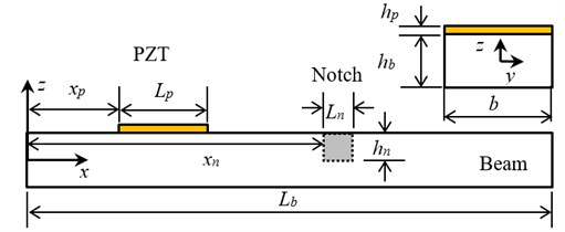
Fig. 3The meshing diagram for the SFEM model
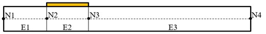
a) Pristine beam
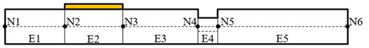
b) Notched beam
A commercialized AD5933 evaluation board was used in the experimental setup for the impedance measuring, as shown in Fig. 4. The evaluation software of Analog Devices (Analog Devices, Inc., 2009) is used to run the board and to send/receive signals. The built in discrete Fourier transform module enable us to extract the real and imaginary part of the measured impedance data at each output frequency.
Fig. 4Experimental setup for measuring electromechanical impedance
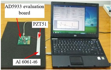
Fig. 5Comparison of the EMI obtained by SFEM, experiment, and FEM
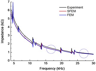
The electromechanical impedance in a frequency range of 4-30 kHz, which obtained by the SFEM, FEM and experiment, respectively, are shown in Fig. 5, also the nature frequencies caculated by SFEM are listed in Table 2, which demostrated that the resonance peaks in the EMI curves corresponding well with the nature frequencies. As the structure undergo a large deformation in resonance state, which result a greater deformation and electric displacement of PZT wafer, eventually leads to a corresponding peak in the impendence curves. It can also be seen that frequency and amplitude of resonance peaks obtained by SFEM and FEM are exactly close. Although the impedance spectra obtained by SFEM is slightly lower than that by the experiment, the overall trend is consistent. The difference may be caused by the slight difference between the material parameters that adopted in numerical simulation and the actual parameters in the experiment. Therefore, it can be concluded that the SFEM is an efficient tools for the numerical analyzing of the electromechanical impedance responses of a coupled piezoelectric beam.
Table 1Material properties of aluminum beam and PZT
PZT51 | Al 6061-t6 | |
Stiffness coefficient (GPa) | 75.99 | |
Piezoelectric constant (V/m) | –7.561×10⁸ | |
Dielectric constant (m/F) | 6.131×10⁷ | |
Density (kg/m3) | 7450 | 2800 |
Young’s modulus (GPa) | 69 |
Table 2The natural frequencies of the model in Fig. 2 between 4 kHz and 30 kHz
Mode No. | 8 | 9 | 10 | 11 | 12 | 13 | 14 | 15 | 16 | 17 | 18 |
(kHz) | 4.679 | 6.497 | 8.592 | 11.04 | 11.86 | 13.71 | 16.53 | 19.84 | 23.21 | 24.00 | 26.73 |
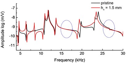
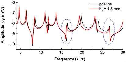
To study the influences of the damage on the electromechanical impedance signal, the electromechanical impedances spectra of the beam-PZT coupled structure with different notch depth ( 0.5 mm, 1 mm and 1.5 mm) obtained by experimental and theoretical are shown in Fig. 6(a) and (b), respectively. The simulation results correspond well with the experiment, which further validates the proposed model. The results indicated that most of the resonant peaks of impedance shift towards left with the increasing of the notch depth. The decrease of the resonant peaks frequencies, which reflect the decreasing of local stiffness, is caused by the existence of local damage (notch). Therefore, the amount of frequency shift increase with the increasing of the notch depth. However, the resonance frequencies of some certain mode (around 4.6 kHz and 13.7 kHz) nearly remain unchanged. This is because the notch is located near the node of corresponding vibration mode where the displacements are almost zero. According to the above analysis, the range of sweeping frequency must be carefully chosen to contain adequate resonant peaks and reject those “unchanged” peaks in order to improve the accuracy of damage identification in practical tests.
Fig. 6Electromechanical impedance of the specimen beam
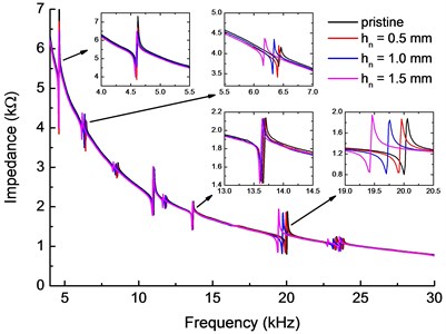
a) Experimental
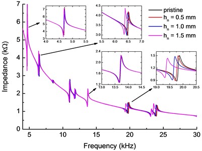
b) Theoretical
Based on the model shown in Fig. 2, frequency response functions (FRFs) on the right free end of the undamaged beam and the notched beam ( 1.5 mm) are also obtained. Displacement amplitudes vs. frequency in the range of 4-30 kHz are presented in Fig. 7. The results show that the FRFs spectra of the axial displacement have almost the same resonance frequencies with the impedance spectra, as well as the frequency shift caused by the notch. The damage caused FRFs variation is the internal reasons of the impedance variation, which can be directly measured in the practical test. In addition, there are some resonance frequencies of vertical displacement (marked with dashed circle in Fig. 7(b)) doesn’t correspond to a peak of axial displacement and impedance spectra. This is because the coupling effect between PZT wafer and the beam is conceded only in -direction, thus the electromechanical impedance is more sensitive to the axial vibration of the beam.
Fig. 7FRFs at the right free end of the beam described in Fig. 2
a) Axial displacement (-direction)
b) Vertical displacement (-direction)
Table 3Material properties of aluminum beam and PWAS varying with temperature
PZT51 | Al 6061-t6 | |||
Stiffness coefficient (GPa) | 75.99 | 4.525×10⁻³ | ||
Piezoelectric constant (V/m) | –7.561×10⁸ | –4.368×10⁵ | ||
Dielectric constant (m/F) | 6.131×10⁷ | 4.153×10³ | ||
Density (kg/m3) | 7450 | –0.0726 | 2800 | –0.1844 |
Young’s modulus (GPa) | 69 | –0.0262 | ||
Previous research has shown that the temperature effects may reduce the efficiency and reliability in the application of EMI [20]. To study the influence of the temperature effects on the impedance of the PWAS sensor, a linear dependence of the material property on temperature is assumed:
where represents one of the material parameter, is the generic temperature, is the reference temperature 25 °C, and is the temperature variation relative to the reference. The parameters of aluminum beam and PWAS in this study are listed in Table 3.
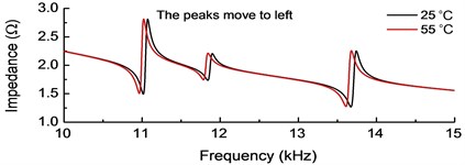
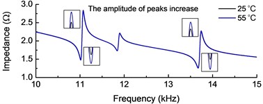
The electromechanical impedance spectra at different temperatures (25-55 °C) have been shown in Fig. 8. It shows that the frequencies of the resonant peaks shift towards left while its amplitude increases with the increasing of temperature. To further analyses the effect of different factors on the impedance signal, the impedance spectra are shown in Fig. 9 (a) with only the beam parameters considered as functions of temperature while the PZT wafer parameters are constant. It can be drawn that the left shift of the impedance resonance peaks is obvious as the temperature rises, while the amplitude change is not so apparent. This is because the structure stiffness decrease with the increase of temperature, which decrease the resonance frequency of the beam. Fig. 9(b) presents the impedance spectra with only the PZT wafer parameters changes with temperature. It is shown that the amplitude of resonance peaks increases without significant left shift, which is mainly contribute to the increase of piezoelectric coefficient of the PZT wafer. Therefore, with the increase of temperature, the left shift of the impedance resonance peaks is mainly due to the parameters changes of the beam, while the increase in impedance amplitude is principally due to the changes of PZT wafer parameters.
Numerical simulation studies have revealed the influence of the damage and temperature variation on the impedance spectra while the results are consistent well with the existing experiment [23]. The results also show that the proposed model has the capability of capturing the changes of impedance with considering the variation of structural/PZT wafer parameters caused by temperature effect, which is unavoidable for real time and online SHM. Many researchers have proposed temperature compensation strategies by results correction to improve the damage detecting precision. The effectiveness of these methods was proved by numerical simulation results in this study.
Fig. 8Electromechanical impedance curves for different temperatures (25-55 °C) considering PZT wafer and beam parameters change with temperature variation
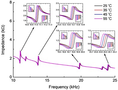
Fig. 9Electromechanical impedance curves for different temperatures only considering a) beam or b) PZT wafer material parameters change with temperature variation
a)
b)
5. Conclusions
Numerical model based on the spectral element method are established to predict the electromechanical impedance spectra of the PZT wafer bonded to the beam, only a small number of spectral elements are required for the accurate computation of the coupled dynamic responses. The high efficiency and accuracy of the spectral element model is validated first by FEM and experiments. The results show that the frequency of the resonance peaks left shift strongly depends on the location and depth of the notch. When the notch is located at a modal node, the corresponding frequency value will remain unchanged. If the notch is away from the modal node, the frequency shift would be significant. Further, the monotonic left shift of resonance peaks may also cause by temperature increasing. The higher the frequency, the greater the deviation will arise. The results show that the proposed numerical model has the capability of capturing the effect of damage and temperature variation, while the existence of damage can be detected by evaluating the electromechanical impedance signals.
References
-
Zhou W., Li H., Yuan F.-G. Guided wave generation, sensing and damage detection using in-plane shear piezoelectric wafers. Smart Materials and Structures, Vol. 23, Issue 1, 2014, p. 15014.
-
Lim Y. Y., Soh C. K. Electro-mechanical impedance (EMI)-based incipient crack monitoring and critical crack identification of beam structures. Research in Nondestructive Evaluation, Vol. 25, Issue 2, 2014, p. 82-98.
-
Xu D., Banerjee S., Wang Y., Huang S., Cheng X. Temperature and loading effects of embedded smart piezoelectric sensor for health monitoring of concrete structures. Construction and Building Materials, Vol. 76, 2015, p. 187-193.
-
Liang C., Sun F. P., Rogers C. A. Electromechanical impedance modeling of active material systems. North American Conference on Smart Structures and Materials, International Society for Optics and Photonics, 1994.
-
Sun F. P., Chaudhry Z., Liang C., Rogers C. Truss structure integrity identification using PZT sensor-actuator. Journal of Intelligent Material Systems and Structures, Vol. 6, Issue 1, 1995, p. 134-139.
-
Park G., Cudney H. H., Inman D. J. Impedance-based health monitoring technique for massive structures and high-temperature structures. Symposium on Smart Structures and Materials, International Society for Optics and Photonics, 1999.
-
Giurgiutiu V., Bao J., Zhao W. Piezoelectric wafer active sensor embedded ultrasonics in beams and plates. Experimental Mechanics, Vol. 43, Issue 4, 2003, p. 428-449.
-
Bhalla S., Soh C. K. Electromechanical impedance modeling for adhesively bonded piezo-transducers. Journal of Intelligent Material Systems and Structures, Vol. 15, Issue 12, 2004, p. 955-972.
-
Yang Y., Lim Y. Y., Soh C. K. Practical issues related to the application of the electromechanical impedance technique in the structural health monitoring of civil structures: I. Experiment. Smart Materials and Structures, Vol. 17, Issue 3, 2008.
-
Yang Y., Lim Y. Y., Soh C. K. Practical issues related to the application of the electromechanical impedance technique in the structural health monitoring of civil structures: II. Numerical verification. Smart Materials and Structures, Vol. 17, Issue 3, 2008.
-
Hamzeloo S. R., Shamshirsaz M., Rezae S. M. Damage detection on hollow cylinders by electro-mechanical impedance method: experiments and finite element modeling. Comptes Rendus Mecanique, Vol. 340, Issue 9, 2012, p. 668-677.
-
Lee U., Kim J., Leung A. Y. The spectral element method in structural dynamics. The Shock and Vibration Digest, Vol. 32, Issue 6, 2000, p. 451-465.
-
Doyle J. F. Wave Propagation in Structures: Spectral Analysis Using Fast Discrete Fourier Transform. Springer-Verlag, New York, 1997.
-
Peairs D. M., Inman D. J., Park G. Circuit analysis of impedance-based health monitoring of beams using spectral elements. Structural Health Monitoring, Vol. 6, Issue 1, 2007, p. 81-94.
-
Wang X., Tang J. Damage identification using piezoelectric impedance approach and spectral element method. Journal of Intelligent Material Systems and Structures, Vol. 20, Issue 8, 2009, p. 907-921.
-
Park H. W., Kim E. J., Lim K. L., Sohn H. Spectral element formulation for dynamic analysis of a coupled piezoelectric wafer and beam system. Computers and Structures, Vol. 88, Issue 9, 2010, p. 567-580.
-
Lee U. Spectral Element Method in Structural Dynamics. John Wiley and Sons. 2009.
-
Sun F. P., Chaudhry Z. A., Rogers C. A., Majmundar M., Liang C. Automated real-time structure health monitoring via signature pattern recognition. Smart Structures and Materials, International Society for Optics and Photonics, 1995.
-
Park G., Kabeya K., Cudney H. H., Inman D. J. Impedance-based structural health monitoring for temperature varying applications. JSME International Journal Series a Solid Mechanics and Material Engineering, Vol. 42, Issue 2, 1999, p. 249-258.
-
Bhalla S., Naidu A. S., Soh C. K. Influence of structure-actuator interactions and temperature on piezoelectric mechatronic signatures for NDE. Smart Materials, Structures, and Systems, International Society for Optics and Photonics, 2003.
-
Gupta V., Sharma M., Thakur N., Singh S. Active vibration control of a smart plate using a piezoelectric sensor-actuator pair at elevated temperatures. Smart Materials and Structures, Vol. 20, Issue 10, 2011, p. 105023.
-
Glushkov E., Glushkova N., Eremin A., Giurgiutiu V. Low-cost simulation of guided wave propagation in notched plate-like structures. Journal of Sound and Vibration, Vol. 352, 2015, p. 80-91.
-
Baptista F. G., Budoya D. E., de Almeida V. A., Ulson J. A. C. An experimental study on the effect of temperature on piezoelectric sensors for impedance-based structural health monitoring. Sensors, Vol. 14, Issue 1, 2014, p. 1208-1227.
About this article

This research was supported by the National Natural Science Foundation of China (Grant No. 11172114), Key Science Research Project of Jiangsu Province (Grant No. BE2015138), the Six Talents Peak Foundation of Jiangsu Province (Grant No. 2012-ZBZZ-027), the National Natural Science Foundation of China of the Key International Cooperation Project (11520101001) and the Research Innovation Program for College Graduates of Jiangsu Province (Grant Nos. KYLX15_1045, KYLX15_1046).
