Abstract
Printed Circuit Boards (PCBs) are epoxy resin-impregnated and cured sheets of counter woven glass fabric (e.g. FR4) laminated between thin sheets of Copper. The nature of the PCB is inherently anisotropic and inhomogeneous but previous modal FEMs of PCBs have assumed isotropic, anisotropic (transversely isotropic and orthotropic) material properties and shown good correlation with test data for specific scenarios [1-3]. This paper details part of a research program aimed at gaining a better understanding of accurately modeling PCB’s dynamic behavior. New investigations into the impact of material anisotropy and, in particular, the effect of material orthogonal plane definition ( and ) on eigenfrequencies is analysed. A modal FEM of a JEDEC PCB is created, verified, and validated using well established theories by Steinberg and empirical data by others [4, 5]. The relative contributions of , and on PCB eigenfrequencies is examined using a parametric modal FEM, analysing the role of material isotropy verses anisotropy. The impact of transversely isotropic material properties is also analysed for a typical JEDEC PCB. This analysis details the mesh density required for accurately modeling the PCB eigenfrequencies. The results show that a 100 % increase in has only a 0.2 % difference in the eigenfrequency where as a 100 % increase in has a 1.2 % difference in the eigenfrequency. The effect of orthotropic plane definition (alternating with ) on the JEDEC PCB amount to a 7.95 % delta in eigenfrequency.
Highlights
- Role of PCB material anisotropy has been investigated using modal FEA.
- Mesh density required to accurately model PCB eigenfrequencies is predicted.
- Critical parameters have been highlighted for PCB eigenfrequency prediction, specifically Young’s modulus.
- FEA model created can be used to determine the PCB’s response to different load environments.
1. Introduction
New trends in heterogeneous integration of electronic ICs has led to increased design complexity and decreases in design margins. This era of IC development is commonly called More than Moore (MtM) or Beyond Moore’ s Law [6]. These electronic packages are commonly used in industries with rugged environments, such as the Space industry, and are subject to a set of system level acceleration load cases. Common test load cases include Random Vibration Acceleration Spectral Density (ASD) and Shock Response Spectrum (SRS). Knowledge of the electronic PCB dynamic behavior is critical to the evaluation of the response to these environmental loads and survivability of the IC packages.
Predicting the eigenfrequencies of the PCB using modal Finite Element Analysis (FEA) can allow for the estimation of PCB component fatigue life for a given electronic package using Steinberg criteria for Random ASD and SRS. Further analysis using techniques from the same author predicts minimum eigenfrequency required to sustain 20 million stress reversal cycles and ideal electronic chassis eigenfrequency to octave decouple PCB modes with the chassis [5]. During the preliminary design phase, it is necessary to carry out structural analysis of the multi-layer PCBs and their components. Estimation techniques are employed to derive approximate elastic material properties [7] and inclusion of discrete components as mass/stiffness adjustments to the PCBs [3]. Other FEM reduction methods include the assumption of linear elastic isotropic properties [8]. It is common design practice that final manufactured designs undergo sine sweep modal response testing and modal analysis discrepancies are accounted for by using reverse FEA and typically updating the Young's and shear moduli [9]. However, at this point in the design, unfavorable responses or performance can cause an expensive, time-consuming and resource intensive redesign. Accurate FEM input parameters are therefore essential.
2. PCB material property
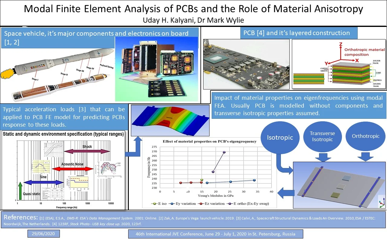
PCBs are broadly available in three types, i.e. single layer, double layer and multi-layer PCBs. The PCB has core material made up of rigid fiberglass and alternate layers of Copper and prepreg. Fig. 1. shows the general PCB board layout consisting of core, prepreg and thin Copper layers. Alternating layers of prepreg comprises of either fill or warp fibers. The fill direction fibers are given a 0° orientation whereas the warp fibers are given a 90° orientation [10]. Typical material property values are given below in Table 1.
Fig. 1Six layer, two-sided PCB construction
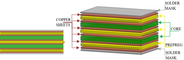
Table 1Material properties of JEDEC standard PCB from literature
Material property | Author 1 [2] | Author 1 [11] | Author 2 [7] |
(Pa) | 1.5E + 10 | 1.69E + 10 | 1. 9E + 10 |
(Pa) | 1.5E + 10 | 1.69E + 10 | 2.3E + 10 |
(Pa) | 1.5E + 10 | 0.74E + 10 | 0.4E + 10 |
(Pa) | Derived from and as 0.53E + 10 | 0.76E + 10 | 1.97E + 10 |
(Pa) | 0.33E + 10 | 1.97E + 10 | |
(Pa) | 0.33E + 10 | 1.97E + 10 | |
0.39 | 0.11 | 0.1 | |
0.39 | 0.39 | 0.4 | |
0.39 | 0.39 | 0.38 | |
Mass density (kg/m3) | 1910 | 1910 | 1900 |
2.1. Modal analysis governing equations
For linear elastic materials obeying Hooke’s law, the Eq. (1) shows the general form of the matrix equation [12]:
where is the mass matrix, represents displacement and , are first (velocity) and second (acceleration) derivative of the displacement. and denote damping factor and stiffness of the system respectively, whereas is force vector. The damping factor is neglected when studying the modal response of a system under free vibration, i.e. undamped frequency is being studied (independent of force) which reduces Eq. (1) as shown below:
The natural frequency for a bare PCB can be theoretically calculated using the Eq. (3):
where and is given as:
where is Young’s modulus (Pa), is the PCB thickness (m), is the length of the free edge (m), is the Poisson’s ratio and is area density (Kg/m2).
Eq. (3) is based on the Rayleigh method and assumes that if no energy is dissipated, the strain energy will be equal to the kinetic energy allowing the natural frequency to be approximated. This equation is applicable when clamped boundary conditions are used [5].
3. Modal FEA of PCBs
Different methods have been used by authors to perform modal analysis of PCBs. Modal FEA of PCBs, carried out by Zhang, using isotropic elastic material properties showed close agreement with test data [2]. In other research by Zhang, the author identifies PCB composition as orthotropic and attempts to optimise the critical properties affecting eigenfrequencies [11]. Zhang applies orthotropic properties for PCB but assumes uniform transverse isotropic material properties (). Equivalent material properties of the board-level package are obtained by means of the Taguchi method (process optimisation and noise reduction methods). This study proffers that Young’s modulus in and plane, shear modulus in - plane and density dominate the resultant eigenfrequencies of the PCB.
In a study carried out to determine the mechanical properties of a PCB by Nilesh [7], it is suggested to consider PCB material as orthotropic as it mirrors the actual PCB composition. He highlights that nine elastic constants are essential to define PCB material properties, which consist of Young’s modulus (, and ), shear modulus (, , ) and Poisson’s ratio (, , ) respectively. The results show that varying from 3 GPa to 12 GPa (in the increments of 1 GPa) does not show a significant change in eigenfrequencies. The author considers constant and values ( 19 GPa and 23 GPa) so their effect on eigenfrequencies is not analysed. Also, in-plane Poisson’s ration and shear modulus show higher impact on eigenfrequencies compared to properties in - and - planes.
Fig. 2JEDEC standard PCB layout matched with model of author 1 [2]
![JEDEC standard PCB layout matched with model of author 1 [2]](https://static-01.extrica.com/articles/21446/21446-img2.jpg)
For this research, a JEDEC PCB is considered to allow for the analysis of the effect of change in Young’s modulus material properties on eigenfrequency. The PCB has been modeled with dimensions 132×77×0.9 mm as seen in Fig. 2. The analysis defines clamping fixation using two flat bars at each PCB edge.
4. Method
Model 1: A modal FEM using a populated (three BGAs), edge clamped JEDEC PCB (free, unsupported PCB aspect ratio of 1.35) is created of the experimental set-up by Zhang [2]. Boundary conditions have been estimated based on scaled measurements taken from this paper. Mesh convergence is carried out and a close correlation is achieved with test data eigenfrequency. The validity of Steinberg's equation is examined with this model. Model 2: Using our validated FEM approach, orthotropic material properties according to the literature are applied. The effect of a range of increasing typical values of (+50 % and +100 % increments) is examined on the eigenfrequencies. Model 3: The effect of transverse isotropic material properties is examined by alternating and values. Finally, Model 4 examines the impact of a range of typical (+50 % and +100 % increments) values on the eigenfrequencies. Fig. 3 shows an example of the FEM of the PCB and the boundary conditions.
Fig. 3FEM with boundary conditions (highlighted in blue)
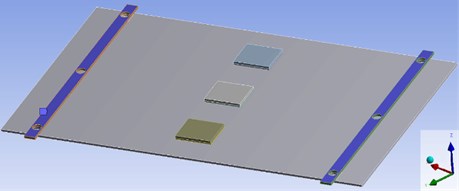
Table 2PCB material properties of four models created for FEM
Material property | Model 1 | Model 2 | Model 3 | Model 4 |
(Pa) | 1.5E + 10 | 1.69E + 10 | 1. 9E + 10 | 2.3E + 10 |
(Pa) | 1.5E + 10 | 1.69E + 10 | 2.3E + 10 | 1. 9E + 10 |
(Pa) | 1.5E + 10 | 0.74E + 10 | 0.4E + 10 | 0.4E + 10 |
(Pa) | Derived from and as 0.53E + 10 | 0.76E + 10 | 1.97E + 10 | 1.97E + 10 |
(Pa) | 0.33E + 10 | 1.97E + 10 | 1.97E + 10 | |
(Pa) | 0.33E + 10 | 1.97E + 10 | 1.97E + 10 | |
0.39 | 0.11 | 0.1 | 0.1 | |
0.39 | 0.39 | 0.4 | 0.4 | |
0.39 | 0.39 | 0.38 | 0.38 | |
Mass density (kg/m3) | 1910 | 1910 | 1900 | 1900 |
5. Results
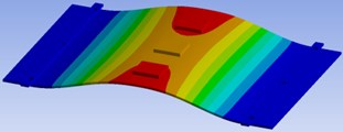
Zhang predicts fundamental frequency of the JEDEC PCB using FEA as 260 Hz, but testing revealed values of 239.5Hz [2]. The linear dynamic FEM of Zhang’s test set up, carried out as part of this research, was found to be 99.8 % accurate (eigenfrequency of 239.02 Hz vs. 239.5 Hz), achieving mesh convergence with a density of 0.63 elements per mm. The mesh consists of 62288 linear hexahedral elements total and mesh quality showing skewness of 95 % elements below 0.25 (in the range of 0-1). The eigenmode shape is shown in Fig. 4.
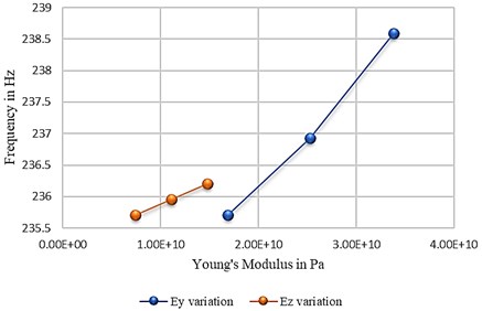
Using Eqs. (3-5) the eigenfrequency is calculated as 246 Hz. The difference in frequency from Steinberg calculation and test (239.50 Hz) is 2.8 %. Using our FEM approach of incrementally increasing values of by 50 % shows a maximum of 0.2 % difference on eigenfrequency (1st mode), see Fig. 5. The range of values are examined for impact on the eigenfrequencies with and are kept constant is studied. This resulted in a maximum of 1.2 % difference on eigenfrequency (1st mode) if the property is increased 100 %, see Fig. 5.
Fig. 4Model 1 eigenmode shape with properties from Table 2
The validity of use of transverse isotropic material properties is examined by alternating and values. It was found that alternating and resulted in an increase in eigenfrequency of 7.95 %, an increase from 247.76 Hz to 269.18 Hz.
Fig. 5Effect of increasing Ey and Ez on PCB’s eigenfrequency
6. Conclusions
This study is aimed at highlighting critical parameters when predicting PCB eigenfrequencies, specifically Young’s modulus. Elastic material properties values are presented for JEDEC PCBs. A FEM of a populated JEDEC PCB test, carried out by others, is validated and shows good correlation using a mesh density of 0.63 elements per mm.
Steinberg’s equation for first eigenfrequency is also found to be applicable and even though it only considers isotropic Young’s modulus material properties, it can closely approximate a PCB with components. This supports the method of omitting discrete electronic components from the modal FEM and instead including them as a mass/density adjustment smeared across the PCB volume. The equation is valid for a simple clamped configuration but perhaps not for a PCB mounted via stand-offs as first eigenfrequency will take contributions from and . has been shown to have minimal impact on the eigenfrequency and highlights this model case as an effective plane stress condition. Assigning the correct in-plane material property values (, ) is essential and will affect the modal FEM results. The orthogonal definition of the PCB and material property assignment is more likely to have a significant impact on eigenfrequencies if the PCB aspect ratio is greater.
References
-
Taek Y. O., Hyun S. S., Young H. K., Yoon H. K. The dynamic characteristic of printed circuit board with the use of the concept of simplified representative elements. JSME International Journal, Vol. 49, Issue 4, 2006, p. 965-972.
-
Bo Z., Han D., Xin Jun S. Modal analysis of board-level electronic package. Microelectronic Engineering, Vol. 85, Issue 3, 2008, p. 610-620.
-
Thraza Mary M., Dash P. K., Kodavanla B. Modelling and simulation of effect of component stiffness on dynamic behaviour of printed circuit board. International Journal of Mechanical and Production Engineering Research and Development, Vol. 8, Issue 2, 2018, p. 307-314.
-
Liangjun X., Hui W. Research on dynamic model of printed circuit board based on finite element method. AIP Conference Proceedings, USA, 2017.
-
Steinberg D. S. Vibration Analysis for Electronic Equipment. 3rd Ed., John Wiley & Sons, New York, 2000.
-
Hengyun Z., Faxing C., Tingyu L., Wensheng Z. Modeling, Analysis, Design, and Tests for Electronics Packaging beyond Moore. Woodhead Publishing, Duxford, 2019.
-
Bhavsar N. R., Shinde H. P., Bhat M. Determination of mechanical properties of PCB. International Journal on Mechanical Engineering and Robotics (IJMER), Vol. 2, Issue 4, 2014, p. 23-27.
-
Guoquan R., Ben L., Dongwei L., Yingqi J. Modal analysis of the printed circuit board based on finite element method. International Conference on Computer Science and Electronic Technology, ShenZhen, 2014.
-
Alastair Amy R., Aglietti G. S., Richardson G. Accuracy of simplified printed circuit board finite element models. Microelectronics Reliability, Vol. 50, Issue 1, 2010, p. 86-97.
-
Qi Z., Shrotriya P., Sottos N. R., Geubelle P. H. Three-dimensional viscoelastic simulation of woven composite substrates for multilayer circuit boards. Composites Science and Technology, Vol. 63, Issue 13, 1971, p. 1983-2003.
-
Bo Z., Pin Kuan Liu, Han Ding, Wenwu Cao Modeling of board-level package by finite element analysis and laser interferometer measurements. Microelectronics Reliability, Vol. 50, Issue 7, 2010, p. 1021-1027.
-
Clough R. W., Penzien J. Formulation of the MDOF Equation of Motion. Dynamics of Structures, McGraw-Hill Publishing Company, New York, 1995, p. 173.
Cited by
About this article

