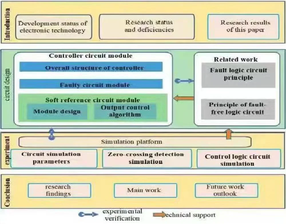
Abstract
The basic idea of the circuit fault diagnosis method based on fault logic is to establish a computer expert database system first, connect the computer to the GPIB interface card, and then connect each intelligent instrument through the GPIB standard bus. Through the connection of the tested object adapter and the tested object, a circuit fault expert diagnosis and test platform are formed. Based on the traditional fault simulation model, this paper improves the fault logic circuit of switching power supply, designs the system model of fault simulation, deals with the logic structure and circuit hierarchy respectively, and produces the final output through the logic gate circuit by comparing the results of the fault logic circuit and the fault-free logic circuit. The designed switching power supply fault logic circuit works in the switching state, which has the characteristics of low loss and high energy conversion efficiency. Through the simulation analysis, the output is connected to the comparator, which plays the role of the whole wave. The simulation results are in line with the parameter indicators. The functional test results of the chip show that the function of the module is basically normal, which has practical application value and good portability and can be used as a reference for similar electrical designs.
Highlights
- A system model of fault simulation was designed.
- Hierarchical processing on that logic structure and the circuit was carried out.
- The control logic circuit is modeled by using the state space.
1. Introduction
With the advent of artificial intelligence (AI), the Internet of Things (IOT) and the 5G era, electronic information technology has developed rapidly. The manufacturing technology of electronic components such as integrated circuits has become more and more advanced. The electronic equipment has gradually developed towards miniaturization and modularization, and the demand for power supply has also developed towards low-voltage and high-current. This requires that the power supply equipment can not only meet the needs of low voltage and large current but also achieve multi-voltage output [1].
To realize the multi-channel output of the power supply, a plurality of independent power supplies with different output voltages are combined to form a multi-output power supply. However, the power supply formed in this way is essentially the superposition of multiple power supplies, and the components, size, and weight used are the superposition of multiple devices. The cost of this method is high, and it cannot be small and light. Because of the different oscillation frequencies of different power supplies, it will also produce mutual electromagnetic interference [2]. Therefore, this method is not suitable for today's green power application environment.
With the advantages of small size, high efficiency, and wide input and output voltage range, the switching power supply has become the mainstream power supply technology [3]. According to whether the input and output of the switching converter are isolated or not, the switching converter can be divided into two categories: isolated and non-isolated. The isolated converter has a transformer structure. Therefore, multiple outputs can be achieved by winding multiple windings on the transformer [4]. This method not only solves the problem of electromagnetic interference caused by different power supply oscillation frequencies, but also greatly reduces the use of components, reduces the cost, and adapts to the development direction of miniaturization and lightweight of the switching power supply [5].
The early synchronous rectification technology is mainly used in non-isolated switching power supplies, such as buck converters, boost converters, and so on. With the development of synchronous rectification technology, the performance of synchronous rectification MOSFET has been improved and the price has been reduced. At present, synchronous rectification technology has become mature [6]. Nowadays, the research of synchronous rectification technology mainly focuses on the research-based on new materials such as GaN and SiC [7]. Reference [8] is based on SiC synchronous rectification MOSFET and adopts dynamic rectification control to achieve low switching loss and high turn-off voltage up to 1700 V. Reference [9] discusses the research on the turn-on voltage drop and switching loss of the synchronous rectification MOSFET with Trench channel structure, and analyzes the prospect of mass production of the MOSFET with Trench channel structure. In recent years, ROHM has successfully mass-produced the synchronous rectification MOSFET with a double Trench channel structure, which has extremely low turn-on voltage drop and high withstand voltage value up to 1.2kV [10]. Thanks to advanced semiconductor process technology, today’s power MOSFETs can achieve on-state resistances below 2 mΩ, gate charges below 25 NC, and switching frequencies above 50 MHz [11]. Synchronous rectification technology has also been applied in various isolated switching power supply topologies, such as forward converter, flyback converter, half-bridge converter, full-bridge converter, and so on [12].
Switching power supply has many incomparable advantages over traditional linear regulated power supply, and has been widely used in many fields in recent years. The nonlinear system has three different working modes. Thus, it is difficult to model. In order to model the nonlinear system such as Buck converter, it is usually linearized to obtain its analytical solution. In this paper, a pulse frequency modulated quasi-resonant controller is designed and fabricated in ASMC 4 μm/40 V Bipolar process. The simulation, layout, tape-out, functional test, and DEBUG of the chip are completed. Based on this controller chip, a DC/DC switching power supply based on the soft-switching technology is designed, and the corresponding system simulation and verification are completed. The main innovations of this paper are:
The whole circuit of the DC/DC switching power supply based on the soft-switching technology is designed, and the topology of QRCs and PFM control mode is adopted.
The soft reference circuit module designed in this paper has the functions of soft start, restart delay, and precision reference voltage reference, and has a complete control function, which realizes the actual control of the soft reference circuit.
According to the actual selection of the counting-type DPWM, the PWM resolution was determined. Compensation analysis was done to the PID control algorithm. This paper selects the discrete position PID to realize and uses the ZN method to tune the parameters, which provides a basis for the system design based on FPGA digital control.
2. Related work
2.1. Principle analysis of fault logic circuit
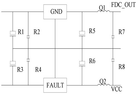
(1) Fault comparator.
The circuit structure of the fault comparator is shown in Fig. 1, and its ports are described as follows:
1) FAULT: Fault signal input (from the system).
2) FDC_OUT: Fault comparator output (connected to VIN_FDC terminal of the fault logic circuit).
As shown in Fig. 1, the 5 V power supply terminal is divided by two resistors and to obtain a 3 V reference voltage. The FAULT terminal signal and the 3V reference voltage are input to a comparator [13] composed of and through an emitter follower respectively. When the input voltage at FAULT is higher than 3 V, and are turned on, and are turned off, and FDC_OUT outputs high; when the input voltage at FAULT is lower than 3 V, and are turned off, and are turned on, and FDC_OUT outputs low [14].
Fig. 1Fault comparator circuit diagram
(2) Fault logic circuit.
The relationship between the fault logic circuit and the soft reference circuit module is shown in Fig. 2, and the fault logic circuit is shown in Fig. 3.
Fig. 2Module relationship diagram of fault logic circuit and soft reference circuit
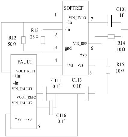
The ports are described as follows:
1) VIN_5 V: 5 V power supply terminal.
2) VIN_FDC: input port (fault comparator FDC_OUT port).
3) UVLO: input port (UVLO port for undervoltage lockout).
4) SOFTREF: the soft reference pin of the chip is externally connected with a 0.1 uF capacitor to the ground.
5) VOUT_LOGIC: output port (monostable pulse generator VIN_AULT port).
Fig. 3Fault logic circuit diagram
2.2. Principle analysis of fault-free logic circuit
During normal operation (no fault generated), the VIN_UVLO terminal is low [15]. When there is no fault signal in the system, it can be seen from the above analysis that the VIN_FAULT1 and VIN_FAULT2 terminals are at high level. At this point, turns off, causing , , and to all turn off. and are also turned off. is turned on, the current mirror formed by and is also turned on, and the current bias circuit works. The SOFTREF terminal of the external capacitor is charged by the power supply voltage through the branch of and until the voltage of the SOFTREF terminal is clamped at 5 V by the clamping circuit [16].
How the 4 V comparator works: When the VIN_FAULT1 terminal is high, is powered down and the 4 V comparator does not work. is on when the VIN_FAULT 1 terminal is low. If the SOFTREF terminal voltage is higher than 4 V at this time, is turned off; if the SOFTREF terminal voltage is lower than 4 V at this time, is turned on. The SOFTREF is charged by the branch where and are located, the voltage of SOFTREF increases, and the collector voltage of also increases [17]. When the SOFTREF terminal voltage is charged to about 4 V, enters the saturation region. is turned on. is turned on. The base level is pulled low. is turned off, and then the 4 V comparator does not work [18].
Working principle of the 0.2 V comparator: during normal operation, the voltage at the SOFTREF terminal is about 5 V. is turned off, and the level at the VOUT_FAULT terminal is low; in case of a fault, the SOFTREF terminal discharges through the , , and loops, and the voltage at the SOftREF terminal gradually decreases. When the voltage at the SOFTREF terminal drops to 0.2 V, is turned on. The level at the VOUT_FAULT terminal changes from low to high, acting on the fault module circuit [19]. When is off, the emitter potential of is given by:
When the VIN_FAULT terminal level goes from low to high, the VIN_REF terminal level also goes from low to high. It can be seen from the above analysis that in the previous state of the circuit, the base level of is high. The base level of is high. The terminal level of VOUT_LOGIC is high, and the terminal levels of VOUT_REF1 and VOUT_REF2 are low. If the VIN_REF level changes from low to high, is turned on. The base level of goes from high to low. The base level of goes from high to low. The level of VOUT_LOGIC goes from low to high, and the levels of VOUT_REF1 and VOUT_REF2 go from low to high [20].
In summary, during normal operation, the 5 V power supply charges the SOFTREF terminal, and the voltage of the SOFTREF terminal gradually increases from 0 to 5 V, and then remains unchanged; the system generates a fault signal, and the SOFFREF terminal begins to discharge, and recharges when it discharges to 0. 2 V. During the recharging process, when the voltage at the SOFTREF terminal does not reach 4 V, a fault signal is generated [21]. At this time, the voltage at the SOFTREF terminal will continue to charge until it is charged to 4 V and then discharged again until it is discharged to 0.2 V and then charged again until it reaches 5 V, after which it remains unchanged [22].
3. Controller circuit module simulation
After the integrated circuit design is completed, the front-end simulation and verification is the basis to ensure the function and performance of the chip. To manufacture a usable chip, layout design and back-end simulation and verification are also needed. Layout is an indispensable step to manufacture a circuit into a chip, and the quality of layout design will seriously affect the performance of the finished chip. Therefore, in the layout design, it is necessary to reduce the influence of parasitic effects through reasonable placement and routing. For circuits with high performance requirements, layout design should consider matching, noise interference, overcurrent capability and so on.
3.1. Controller overall structure simulation
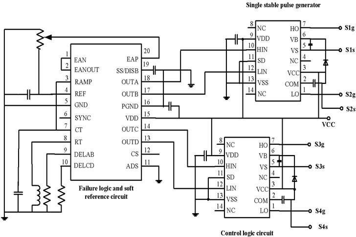
For the overall architecture of the chip, the controller chip is composed of multiple circuit modules, as shown in Fig. 4.
Fig. 4Overall architecture of the chip
Based on the ASMC 4 μm/40 V Bipolar process, the circuit is simulated and verified by using the Cadence Spectre software platform. Process angles (TT/SS/FF), supply voltages (12 V/20 V), and temperatures (–55 ℃/25 ℃/125 ℃) are considered. Parameters of peripheral basic components are: 0.1 μF, 86.6 kΩ, 7.15 kΩ, 1 nF, 4.02 kΩ and 200 pF.
The function of the converter depends on the control loop. In the nonlinear closed-loop feedback loop, the Boost converter has an inherent right-half plane zero. The LC produces a pole. The load of the output stage produces a pole and the error amplifier also introduces a pole. There are multiple poles and zeros in the system, and the phase margin of the multi-pole system cannot be guaranteed, which will cause system instability. Therefore, the frequency compensation is needed. An R, C compensation network is connected at the output end of the error amplifier to provide a zero point for the system so as to improve the influence of the output pole on the phase margin. It also ensures that the phase margin of a feedback loop is larger than 60 and improves the stability of the system.
3.2. Failure circuit module simulation
The main function of the fault circuit module is fault detection and fault protection. The module is mainly composed of a fault comparator (FDC) and a fault logic circuit. The function of the fault comparator (FDC) is relatively simple. It mainly compares the input voltage of the FAULT terminal with the 3 V reference voltage to obtain a voltage signal. This signal passes through circuits such as fault logic to control the output of the MOSFET starter. When the input voltage is above the 3 V reference, the output of the FDC is high. When the input voltage is below the 3 V reference, the output of the FDC is low. Fig. 5 is a functional diagram of a fault circuit module.
Fig. 5Function diagram of faulty circuit module
4. Soft reference circuit module simulation
4.1. Soft reference circuit module design
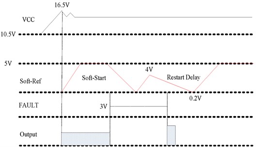
The main functions of the soft reference block are soft start, restart delay, and precision voltage reference. Wherein, the restart delay function needs to be realized in combination with the fault circuit module. Since the circuit function of the soft-reference circuit module is relatively complex, it will be analyzed from the perspective of the soft-Ref pin function in conjunction with Fig. 6.
As shown in Fig. 6, the Soft-Ref pin performs three functions: Soft-Start, Restart-Delay, and Precision Reference (5 V). In undervoltage lockout (UVLO), all outputs are low and the external capacitor on the Soft-Ref pin is discharged. When the supply voltage VCC exceeds the UVLO upper limit, the internal current source charges until it is clamped at 5 V by the 5 V clamp circuit. The soft start time is roughly given by:
In the event of a fault, all outputs are driven low. The external capacitor is discharged by a 20 μA current source. This is the restart delay period. When reaches 0.2 V, the output is enabled and is charged with a 0.5 mA current. If a fault occurs before the end of the charge cycle, the output is immediately driven low, but charges to 4 V before the 20 μA restart delay current discharges . The restart delay time during continuous fault operation is:
Fig. 6Functional diagram of soft reference circuit module
The restart delay function can be removed by adding a 100 kΩ resistor between the Soft-Ref pin and the 5 V pin. In this case, however, the fault detection circuit will permanently shut down the converter in the event of a fault. The converter does not return to normal operation until the VCC is reapplied and the UVLO circuit resets the fault circuit, leaving the external 100 kΩ resistor open. When a 100 kΩ resistor is connected, the soft start time becomes:
The precision reference at the Soft-Ref pin is due to an internal 5 V clamp. A 15 Ω resistor is connected between the Soft-Ref pin and the clamp circuit to avoid the regulated voltage fluctuation caused by the external capacitor.
4.2. Clock frequency output control algorithm
A voltage is taken from the output voltage and fed back to the error amplifier (EA). This feedback signal is compared to a 5 V reference voltage and an error voltage is an output. The error voltage is used as a control voltage to control the oscillation frequency of a voltage-controlled oscillator (VCO), and then a square wave signal is an output through a control logic circuit and an output driving circuit to drive a switch tube to control the working state of a peripheral circuit and finally keep the output voltage stable.
In a ZVS circuit, the output voltage will decrease as the frequency increases. Therefore, in practical applications, the inverting input of the EA should be connected to the reference voltage, and the non-inverting input of the EA should be connected to the feedback voltage.
Control the internal operating frequency, which is controlled by the error amplifier output.
The VCO is externally connected with two resistors and and a capacitor . and determine the minimum frequency:
When the output of the error amplifier is less than or equal to one diode drop, the VCO operates at the minimum frequency. The VCO frequency is at its maximum when the error amplifier output rises one diode drop below 5 V:
The usable frequency range is the difference between the first two equations:
Because the nominal output swing of the error amplifier is approximately 3.6 V due to a full-scale change in the VCO frequency, the gain of the VCO block is as follows:
5. Simulation experiment analysis
5.1. Circuit simulation parameters
For Simulink simulation with ModelSim module, when all configurations are completed, MATLAB can be added to edit and verify the program. It can also make preparations for joint simulation, set the port and clock frequency, simulation accuracy, communication serial port, and set simulation parameters through 53885 for communication. After setting, the module is connected to the Buck circuit topology in Simulink to complete the drawing of Simulink simulation.
The parameter indexes mainly involved in the fault circuit module are shown in Table 1.
Table 1Main parameters of fault circuit module
Parameters | Minimum value | Typical value | Maximum value |
Fault comparator threshold (V) | 2.85 | 3.00 | 3.15 |
Fault to output delay (ns) | – | 100 | 200 |
Table 2Fault comparator thresholds
TT (V) | SS (V) | FF (V) | ||
12 V | –55 °C | 3.0177 | 3.0604 | 2.9843 |
25 °C | 2.9920 | 3.0753 | 2.9412 | |
125 °C | 3.0585 | 3.1101 | 2.9410 | |
20 V | –55 °C | 2.9349 | 3.0753 | 2.9602 |
25 °C | 3.0008 | 3.0726 | 2.9392 | |
125 °C | 3.0372 | 3.1088 | 2.9419 | |
Simulation results of main parameters of the fault circuit module are shown in Table 2 and Table 3 respectively.
Table 3Failure to output delay
TT (ns) | SS (ns) | FF (ns) | ||
12 V | –55 °C | 117.5 | 134.8 | 102.9 |
25 °C | 117.2 | 136.7 | 99.2 | |
125 °C | 137.4 | 161.5 | 112.3 | |
20 V | –55 °C | 122.4 | 150.2 | 107.3 |
25 °C | 121.4 | 141.4 | 103.1 | |
125 °C | 142.1 | 167.0 | 116.7 | |
5.2. Comparison of simulation results for zero-crossing detection
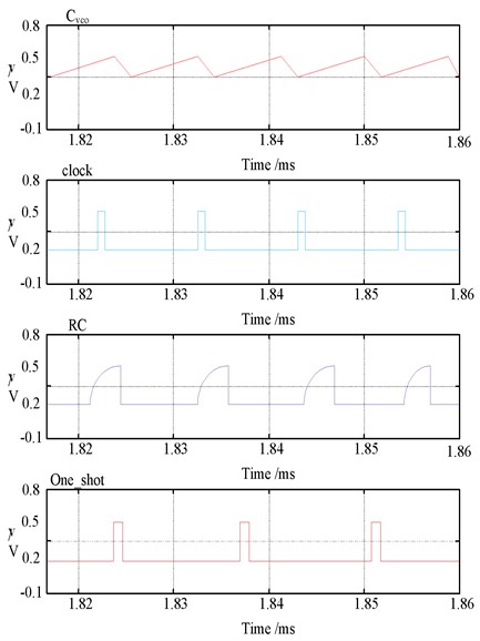
The simulation results of the zero-crossing detection comparison and main parameters of the monostable pulse generator module are shown in Tables 4-6 respectively.
Table 4Zero-Crossing detection comparator thresholds
TT (V) | SS (V) | FF (V) | ||
12 V | –55 ℃ | 0.500 | 0.514 | 0.488 |
25 ℃ | 0.502 | 0.518 | 0.490 | |
125 ℃ | 0.494 | 0.508 | 0.480 | |
20 V | –55 ℃ | 0.500 | 0.516 | 0.488 |
25 ℃ | 0.504 | 0.518 | 0.490 | |
125 ℃ | 0.500 | 0.508 | 0.480 | |
Table 5Maximum pulse width
TT (ns) | SS (ns) | FF (ns) | ||
12 V | –55 ℃ | 1035.0 | 1007.7 | 1079.3 |
25 ℃ | 1000.1 | 1003.6 | 999.4 | |
125 ℃ | 991.5 | 963.8 | 992.2 | |
20 V | –55 ℃ | 1035.1 | 1010.5 | 1079.0 |
25 ℃ | 1000.3 | 1003.6 | 1000.4 | |
125 ℃ | 991.7 | 994.9 | 991.7 | |
Table 6Ratio of maximum to minimum pulse width
TT (ns) | SS (ns) | FF (ns) | ||
12 V | –55 ℃ | 3.61 | 3.90 | 3.25 |
25 ℃ | 3.93 | 3.92 | 3.89 | |
125 ℃ | 4.01 | 3.89 | 3.95 | |
20 V | –55 ℃ | 3.61 | 3.90 | 3.24 |
25 ℃ | 3.92 | 3.92 | 3.90 | |
125 ℃ | 4.01 | 4.02 | 3.95 | |
5.3. Results of the control logic circuit simulation
Fig. 7 is the function simulation waveform diagram of the control logic circuit module.
The parameters mainly involved in the control logic circuit module are shown in Table 7.
Table 7Main parameter indexes of control logic circuit module
Parameters | Conditions | Minimum value | Typical value | Maximum value |
Transmission delay(ns) | — | — | 120 | 200 |
Simulation results of main parameters of the control logic circuit module are shown in Table 8.
Fig. 7Function simulation waveform of the control logic circuit module
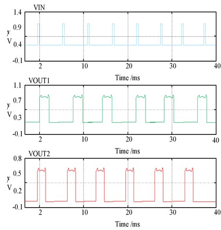
Table 8Transmission delay
TT (ns) | SS (ns) | FF (ns) | ||
12 V | –55 ℃ | 80.2 | 86.3 | 87.6 |
25 ℃ | 50.1 | 54.2 | 60.3 | |
125 ℃ | 52.3 | 73.8 | 52.7 | |
20 V | –55 ℃ | 88.9 | 68.2 | 89.3 |
25 ℃ | 57.7 | 57.4 | 60.3 | |
125 ℃ | 60.3 | 62.4 | 51.9 | |
6. Conclusions
Compared with the traditional linear power supply, the switch tube in the switching power supply works in the switching state, so the loss is small and the energy conversion efficiency is high. In addition, the switching power supply does not need a power frequency transformer, and is small in size and light in weight. Based on the soft reference circuit model, this paper designs the logic fault circuit of switching power supply, which can realize the simulation of circuit fault and provide a reference for detecting circuit design defects. Experiments show that the power supply logic circuit designed in this paper can reduce the overshoot voltage and realize the zero-voltage turn-off of the switch tube. The main research contents of this paper are as follows:
1) A DC/DC switching power supply based on the soft-switching technology is designed in this paper.
2) The proposed control logic circuit is modeled by using state space, and the transfer function of the circuit is further solved on the basis of the established equivalent signal model.
3) Set up the experimental environment and analyze the experimental results, which shows that the parameters basically meet the requirements and verify the rationality of the design.
Because the power converter is a strong nonlinear system, the nonlinear model is linearized to obtain an approximate linear model. In future work, the modeling method needs to be further improved to improve the accuracy of the system model and reduce the error.
References
-
H. Delavaripour, B. Mirzaeian Dehkordi, E. Adib, and H. Abootorabi Zarchi, “Dynamic model development and control for multiple-output flyback converters in DCM and CCM,” International Journal of Circuit Theory and Applications, Vol. 46, No. 6, pp. 1228–1248, Jun. 2018, https://doi.org/10.1002/cta.2467
-
Y.-H. Jung, S.-K. Hong, and O.-K. Kwon, “A low load – and cross-regulation SIDO converter using an adaptive current sensor and LDO regulator with a selectable charge pump for mobile devices,” Analog Integrated Circuits and Signal Processing, Vol. 92, No. 2, pp. 293–301, Aug. 2017, https://doi.org/10.1007/s10470-017-0990-7
-
Z. Xiao, G. Zhao, Y. Wang, H. Wang, and W. Hu, “Adaptive frequency adjustment technique in current mode DC-DC converters for input voltage range extension,” IET Power Electronics, Vol. 12, No. 3, pp. 557–566, Mar. 2019, https://doi.org/10.1049/iet-pel.2018.5415
-
S. Singh, D. Mandal, B. Bakkaloglu, and S. Kiaei, “Low-power/low-voltage integrated CMOS sense resistor-free analog power/current sensor compatible with high-voltage switching DC-DC converter,” IEEE Transactions on Circuits and Systems I: Regular Papers, Vol. 66, No. 6, pp. 2208–2218, Jun. 2019, https://doi.org/10.1109/tcsi.2019.2897049
-
Y. Tsukamoto et al., “Mass production technology of flexible AMOLED displays and improvement of the OLED device characteristics,” in 2019 26th International Workshop on Active-Matrix Flatpanel Displays and Devices (AM-FPD), Jul. 2019, https://doi.org/10.23919/am-fpd.2019.8830624
-
S.-W. Hong, S.-H. Park, T.-H. Kong, and G.-H. Cho, “Inverting buck-boost DC-DC converter for mobile AMOLED display using real-time self-tuned minimum power-loss tracking (MPLT) scheme with lossless soft-switching for discontinuous conduction mode,” IEEE Journal of Solid-State Circuits, Vol. 50, No. 10, pp. 2380–2393, Oct. 2015, https://doi.org/10.1109/jssc.2015.2450713
-
B.-C. Kwak, S.-K. Hong, and O.-K. Kwon, “A highly power-efficient single-inductor bipolar-output DC-DC converter using hysteretic skipping control for OLED-on-silicon microdisplays,” IEEE Transactions on Circuits and Systems II: Express Briefs, Vol. 65, No. 12, pp. 2017–2021, Dec. 2018, https://doi.org/10.1109/tcsii.2018.2815994
-
Y.-Y. Lee, S. Park, J. Park, W. Choe, and J. Kwag, “P-237L: late-news poster: single package DC/DC converter for tablet OLED,” in SID Symposium Digest of Technical Papers, Vol. 48, No. 1, pp. 1449–1451, May 2017, https://doi.org/10.1002/sdtp.11921
-
Y. Liu, R. Sekiguchi, and Y. Sano, “Study on improving precision of analysis of boost ratio and power efficiency of tapped-inductor DC-DC converter circuit,” Electrical Engineering in Japan, Vol. 202, No. 4, pp. 3–20, Mar. 2018, https://doi.org/10.1002/eej.23055
-
W. H. Maciel, J. A. R. Carvalho, and F. L. Tofoli, “A unified modeling approach for DC-DC converters based on the three-state switching cell,” AEU – International Journal of Electronics and Communications, Vol. 88, pp. 30–37, May 2018, https://doi.org/10.1016/j.aeue.2018.03.009
-
S.W. Lee and H.L. Do, “High‐efficiency soft‐switching step‐up DC-DC converter derived from a synchronous boost converter,” IET Power Electronics, Vol. 12, No. 7, pp. 1662–1669, Jun. 2019, https://doi.org/10.1049/iet-pel.2018.5581
-
P. K. Maroti et al., “A Novel 2L-Y DC-DC converter topologies for high conversion ratio renewable application,” in 2017 IEEE Conference on Energy Conversion (CENCON), pp. 323–328, Oct. 2017, https://doi.org/10.1109/cencon.2017.8262506
-
S. R. Rex and D. M. M. S. R. Praba, “Design of PWM with four transistor comparator for DC-DC boost converters,” Microprocessors and Microsystems, Vol. 72, p. 102844, Feb. 2020, https://doi.org/10.1016/j.micpro.2019.07.003
-
X. Wang, Y. Guo, W. Cheng, and M. Leng, “Loop stability analysis of boost circuit under globally dynamic compensation strategy,” The Journal of Engineering, Vol. 2019, No. 16, pp. 1853–1857, Mar. 2019, https://doi.org/10.1049/joe.2018.8741
-
S. Banerjee, A. Ghosh, and S. Padmanaban, “Modeling and analysis of complex dynamics for dSPACE controlled closed‐loop DC‐DC boost converter,” International Transactions on Electrical Energy Systems, Vol. 29, No. 4, p. e2813, Apr. 2019, https://doi.org/10.1002/etep.2813
-
Z. Xiao et al., “An automatic slope compensation adjustment technique for peak-current mode DC-DC converters,” AEU – International Journal of Electronics and Communications, Vol. 110, p. 152860, Oct. 2019, https://doi.org/10.1016/j.aeue.2019.152860
-
V. Radhika, K. Srinivasan, B. B. Sharmila, and V. Rukkumani, “Design of digital pulse width modulator architecture with digital PID controller for DC-DC converter using FPGA,” Analog Integrated Circuits and Signal Processing, Vol. 107, No. 2, pp. 299–307, May 2021, https://doi.org/10.1007/s10470-020-01794-8
-
D.-D. Tran, H.-N. Vu, S. Yu, and W. Choi, “A novel soft-switching full-bridge converter with a combination of a secondary switch and a nondissipative snubber,” IEEE Transactions on Power Electronics, Vol. 33, No. 2, pp. 1440–1452, Feb. 2018, https://doi.org/10.1109/tpel.2017.2688580
-
L.-C. Shih, Y.-H. Liu, and H.-J. Chiu, “A novel hybrid mode control for a phase-shift full-bridge converter featuring high efficiency over a full-load range,” IEEE Transactions on Power Electronics, Vol. 34, No. 3, pp. 2794–2804, Mar. 2019, https://doi.org/10.1109/tpel.2018.2838572
-
V. R. K. Kanamarlapudi, B. Wang, N. K. Kandasamy, and P. L. So, “A New ZVS Full-Bridge DC-DC converter for battery charging with reduced losses over full-load range,” IEEE Transactions on Industry Applications, Vol. 54, No. 1, pp. 571–579, Jan. 2018, https://doi.org/10.1109/tia.2017.2756031
-
R. Kathiresan, P. Das, T. Reindl, and S. K. Panda, “A Novel ZVS DC-DC full-bridge converter with hold-up time operation,” IEEE Transactions on Industrial Electronics, Vol. 64, No. 6, pp. 4491–4500, Jun. 2017, https://doi.org/10.1109/tie.2017.2674583
-
L. Yi, H. Zhu, B. Wang, L. Fang, W. Ma, and X. Liang, “A novel full-soft-switching full-bridge converter with a snubber circuit and couple inductor,” in 2019 IEEE 10th International Symposium on Power Electronics for Distributed Generation Systems (PEDG), pp. 60–64, Jun. 2019, https://doi.org/10.1109/pedg.2019.8807655
About this article

The authors have not disclosed any funding.
The datasets generated during and/or analyzed during the current study are available from the corresponding author on reasonable request.
The authors declare that they have no conflict of interest.
