Abstract
Switch mode power suppliers based on isolated flyback topology have voltage stresses on semiconductor switches caused by transformer leakage inductance. Those voltage stresses have to be mitigated by implementing active or passive clamp preferably with partial leakage energy recovery. In this paper a new integrated semi-active regenerative (lossless) snubber is proposed. The proposed snubber topology is featured by the snubber inductor integrated into the main transformer thus decreasing component count and saving the PCB space. Partial coupling of snubber inductor with a secondary side makes it possible to recover part of the transformer leakage energy directly to the secondary side with potential to increase snubber efficiency. The operation of the proposed snubber is analyzed and simulation results are presented. Interesting is that with the proposed snubber various side effects can be reached like reduction of RMS current in secondary side, ZCS and ZVS modes for secondary side rectifier and primary main switch along with achieved primary goal – voltage stress limitation and transformer leakage energy recovery.
Highlights
- Novel regenerative snubber
- New integrated semi-active regenerative snubber
- Auxiliary inductor is integrated
- Equivalent stage circuits
- Switches operation scheduler
1. Introduction
The improvements in power semiconductors and magnetic components make converters based on flyback topology more efficient and hence make it more attractive to implement flyback topology into practical applications. Flyback topology finds broadening usage due to its low component count, simple schematics, robustness and possibility to provide galvanic isolation. But the main problem with flyback topology are voltage stresses on semiconductor switches caused by flyback transformer leakage inductance. There are number of solutions [1] proposed to limit voltage spikes on a main switch. The most desirable of them would be a non-dissipative snubber for better power efficiency and a cost effective one to keep low cost. The RCD snubber circuits are the simplest and robust solutions but unfortunately cannot match increasing power efficiency requirements [2].
In a scientific literature there are well known active clamp snubbers with regenerative capabilities [3-10]. Active clamp can help effectively recover the transformer leakage energy clamped in snubber capacitor; it can also help to provide zero voltage switching mode for the main power switch [3, 5, 9]. But all of these benefits come with the complexity of an active clamp. Other feature of an active clamp in flyback topology, that it increases current RMS value for a secondary circuit and high current peak for secondary rectifier diode before switch off. Also, active clamp reduces the robustness of a flyback, because the auxiliary clamp switch commutates snubber capacitor to output capacitor through transformer leakage inductance [9].
There are also number of passive non-dissipative snubber circuits for flyback converter [11-19]. These passive snubbers significantly and cost effectively reduce turn off switching losses and regenerate leakage energy from snubber capacitor. They recover energy back to power supply DC bus or store in the magnetizing inductor of a flyback transformer. There are some integrated regenerative circuits [15-18], that offer advantage of reducing component count and circuit simplification. Other advantage of these passive integrated regenerative snubbers is that they can partially recover transformer leakage energy forward to the secondary output, thus can potentially demonstrate higher efficiency. The considered regenerative snubbers work in discontinues conduction mode or resonant mode thus with increased RMS in snubber circuits.
There are also some snubber solutions [20, 21] that are worth to mention. Their idea is quiet straight forward and involves commutation of clamp capacitor to the input to restore transformer leakage energy temporarily caught in that clamp capacitor. The snubber [20] actually exploits the idea of a DC/DC converter that recovers energy from clamp capacitor back to input. It is complicated but potentially has the best recovery efficiency, therefore better suits for high power applications. The snubber [21] is a semi-active one with auxiliary switch that synchronously with the flyback main switch commutates clamp capacitor to an input through an auxiliary inductor. The snubber is simpler but potentially has the same best recovery efficiency as the snubber in [20].
In this paper a novel regenerative semi-active snubber circuit with an auxiliary inductor integrated with a main transformer is proposed [22]. It consists of the voltage spike limiting clamp capacitor to catch most of the leakage energy and a transformer auxiliary winding with auxiliary semiconductor switches to recover most of the energy from clamp capacitor. The auxiliary winding is integrated with the main flyback transformer and connected to the flyback schematic in a way to have stage voltages conformed with main transformer windings. The integration of the snubber inductor with the main transformer reduces components count and safes space on a PCB. The main advantage of the proposed snubber over the snubber in [21] is that it have potential to recover most of the energy to the secondary output, therefore promises higher leakage energy recovery efficiency. The behavior of the proposed solution is dependent on multiple parameters, therefore the desirable snubber properties and its side effects can be achieved through particular realization. The snubber can be designed to operate in non-resonant continues conduction mode (CCM) or discontinues conduction mode (DCM). Therefore, the advantage is that it has reduced RMS currents in the snubber circuits compared to the conventional regenerative LCD snubbers [15-18] with recharging in a resonant way flying capacitor. In this work only one of the promising recover strategies has been analyzed. The simulation has been provided to reveal the advantages of the proposed solution. Stage-by-stage consideration has been given, and equivalent schematics was provided for stages along with principal governing equations where it is needed for better comprehension of stage processes.
2. The proposed regenerative snubber circuit for flyback topology
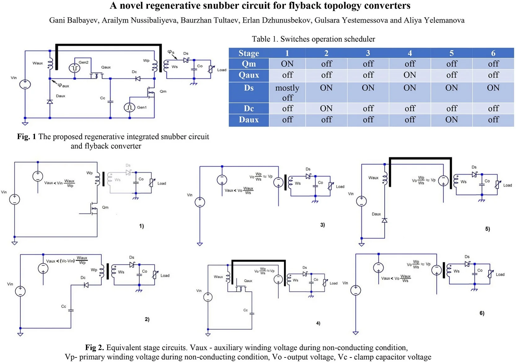
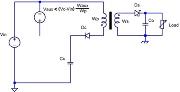
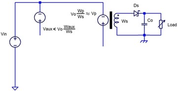
The advantage of the proposed snubber have been achieved by integration of auxiliary inductance with the main transformer, thus the transformer have the third auxiliary winding now. The advantage with this is that the energy can be recovered directly to the secondary output with potential to increase efficiency. The principal schematic of the proposed recovering solution is presented in Fig. 1.
On Fig. 1 one can see a flyback topology converter with a clamp voltage limiter consisting of clamp capacitor and clamp diode , and to drain clamp energy here is the circuit formed by auxiliary transistor , auxiliary diode and auxiliary transformer winding . The auxiliary switch is synchronized with the main switch and can be driven passively or actively. The synchronization and driving of with the main switch can be accomplished by tapping from winding or by means of additional 4th winding. It is clearly seen that the behavior of the circuit is highly dependent on parameters like leakage inductance between transformer windings and auxiliary winding, turns ration / and switching timing parameters of auxiliary transistor . The governing equation system for the proposed three winding transformer looks like Eq. (1):
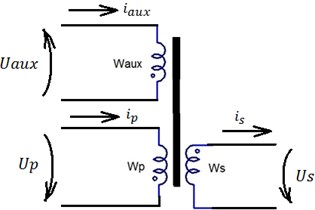
where – transformer primary winding inductance, – transformer secondary winding inductance, – auxiliary winding inductance, – transformer primary to secondary windings mutual inductance, - primary to auxiliary mutual inductance, – secondary to auxiliary mutual inductance. The winding’s current positive directions and voltage drop positive directions on the transformer windings are shown in the Fig. 2.
Fig. 1The proposed regenerative integrated snubber circuit and flyback converter
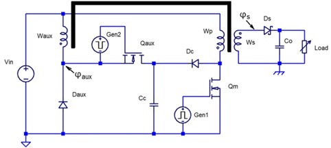
Fig. 2The proposed transformer winding voltages and currents designations and chosen positive directions
We propose to start studying of the schematic on Fig. 1 with some clear assumptions: the auxiliary winding turns number is equal to the primary winding turns number, ; coupling between and other transformer windings is weaker than coupling between primary and secondary windings. For analytical proposes we consider that all semiconductor switches are ideal. We consider the case when auxiliary transistor switches complementary to the main transistor , and here is a delay after switch off and turn on. With these assumptions let’s consider six operating stages in a steady state condition for the circuit on the Fig. 1, and they are all presented in a Table 1.
Table 1Switches operation scheduler
Stage | 1 | 2 | 3 | 4 | 5 | 6 |
ON | off | off | off | off | off | |
off | off | off | ON | off | off | |
mostly off | ON | ON | ON | ON | ON | |
off | ON | off | off | off | off | |
off | off | off | off | ON | off |
The equivalent circuit diagrams are given in Fig. 3 for each of six stages.
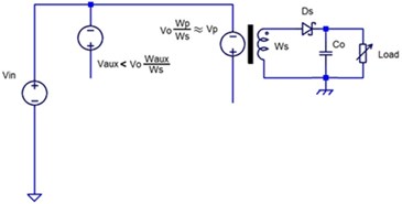
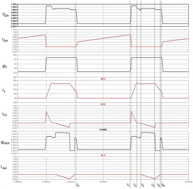
The waveforms have been generated in the simulation software LTspice for the particular circuit parameters: transformer magnetizing inductance 6400 uH, coupling coefficient between primary and secondary windings 0.98, coupling coefficients between auxiliary to primary winding and between auxiliary to secondary windings are both 0.8; switching frequency about 67 kHz; input voltage 400 V, output voltage 14 V and output power 145 W. The duration of the stages and simulated operation waveforms are presented in Fig. 4. From Fig. 4 one can see that in our particular study case the auxiliary winding current flows in discontinues conduction manner. We will consider the case in which the main switch turns on at the time moment after the current in the auxiliary winding calms down to zero. By the moment all primary side semiconductor switches are non-conducting only secondary diode is conducting current to the output helping the flyback transformer to discharge it’s remaining power energy through secondary winding .
Fig. 3Equivalent stage circuits. Vaux – auxiliary winding voltage during non-conducting condition, Vp – primary winding voltage during non-conducting condition, Vo – output voltage, Vc – clamp capacitor voltage
a)
b)
c)
d)
e)
f)
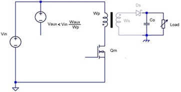
2.1. Stage 1 (-)
In this stage, see Fig. 3(a) main switch is turned on, the transformer primary side is connected to the input mains , the secondary current rapidly goes down. After the output rectifier gets reversed biased the transformer starts to gain power. On Fig. 3(a) the secondary winding and rectifier diode are partially shadowed, because most of the stage time they do not provide any current. At the same time the auxiliary diodes and remain non-conducting. Clamp diode is under reversed voltage of the clamp capacitor . The transformer governing equations at this stage will look like Eq. (2):
On the auxiliary winding here is a reflected voltage from the primary winding , and because in this specific example it happened that thus the voltage applied to the auxiliary diode is near zero. Actually, diode under slight stress of reversed voltage because reflected voltage on is less than input voltage by voltage drop on equivalent primary side leakage inductance. The auxiliary winding is non-conducting, and the auxiliary switch is under stress of clamp capacitor voltage.
Fig. 4Simulation waveforms of the flyback converter circuit with the proposed regenerative snubber. VQm – drain to source voltage on the Qm switch, IQm – current of the Qm switch, φS and φAUX are the potentials of the corresponding nodes on secondary and primary sides (see Fig. 1), Is – current of the secondary side, ICc – current of the clamp capacitor Cc, Iaux – current of the auxiliary winding Waux
2.2. Stage 2 (-)
At the moment the main switch turns off, see Fig. 3(b) and the transformer primary current starts charging clamp capacitor through the diode until transformer leakage energy is depleted, that happens by the time moment . During this stage secondary diode current rises from zero. The transformer governing equations for stage 2 will look like Eq. (3):
The reflected voltage on the auxiliary winding equals to the clamp voltage minus voltage drop on a leakage inductance of the transformer. As the potential of source terminal is lower than the clamp voltage, therefore switch will stay reversed biased and internal diode of as well as diode are remain non conducting. But is under slight reverse voltage thus it is the good moment for switch to turn on. But we will make some longer delay before turns on. The delay duration is optional, and may not last for two stages as we made. As the potential of source terminal is lower than the clamp voltage, therefore internal diode of as well as diode are remain non conducting.
2.3. Stage 3 (-)
Equivalent schematic of this stage is on Fig. 3(c). By the moment the transformer leakage energy is depleted and diode is closed. Here is still some time after the main switch turned off and before the auxiliary switch turns on. During this time interval transformer primary and auxiliary windings are non-conducting, all semiconductors on the primary side are non-conducting. Only transformer secondary side discharges energy gained at stage 1 into output through the diode and the transformer governing equations will look like Eq. (4):
In this short stage current of the secondary side decreases.
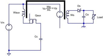
2.4. Stage 4 (-)
At the moment the auxiliary switch turns on in order to discharge the clamp capacitor , Fig. 3(d). Thus, the capacitor discharges directly into secondary side through the coupled windings and , also onto the transformer leakage and transformer magnetizing inductance. The linear current rise on is determined by the leakage inductance, see Eq. (5):
where is the equivalent leakage inductance between auxiliary and secondary sides seen/measured from auxiliary side. Because of the leakage between and primary the reflected voltage on is not big enough to open clamp diode and hence primary winding remain non-conducting. From moment secondary current slows down it’s decrement and in our particular case we can observe some increasing due to energy supply from clamp through auxiliary switch . It is possible to select the value of leakage inductance and duration of stage 3 to make secondary current flat during conduction of the secondary rectifier , from time to , thus RMS current could be reduced. Simulation shows that if we made more time for to be open, for example at the expense of time delay between turn off and turn on (stages 2, 3), then the clamp voltage would be lower due to increased discharge time and secondary current slope would be declining. Also, simulation shows that decreasing the leakage between auxiliary winding and other transformer windings will reduce the clamp voltage as the discharge rate will be faster, will increase peak current for and increase upward slope of the secondary current.
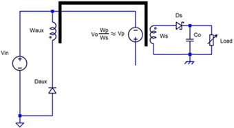
2.5. Stage 5 (-)
During this time period, see Fig. 3(e), the auxiliary switch turns off but here is some delay up to the time moment then the main switch turns on. At the time when switches off auxiliary winding current starts to flow through auxiliary diode until it diminishes to zero. The transformer governing equation for this stage will look like Eq. (6):
Thus, the leakage energy associated with fully discharges back to the input. As a result, the clamp energy fully recovered mostly forward to the secondary output, partly back to the input and partly in the form of transformer magnetizing energy gained at stage 5 from clamp through winding . While current depletes at the same time secondary diode current goes down as current from clamp capacitor no longer feeds secondary output and leakage energy associated with exhausts. Magnetizing current gained at stage 5 also starts to flow in secondary side reducing diode current in forward direction! It is potentially possible to make soft turn-off of the diode and soft turn on of by turning parameters of a transformer, for example it could happen if the flyback topology was closer to the discontinues conduction mode. Delay duration between turn-off and turn-on should be taken as long just to decrease secondary current as much as possible before the main switch turns on. But in our particular case for the research purposes again we made this delay to last for one more additional stage.
2.6. Stage 6 (-)
Equivalent schematic of this circuit is on Fig. 3(f). From the time moment up to the moment both auxiliary and primary windings are non-conducting. All semiconductors on the primary side are switched off. The flyback transformer continues to provide remaining energy to the output secondary side through the diode with descending secondary current:
3. Discussion
The better the coupling coefficient between auxiliary and secondary transformer windings the more portion of the transformer leakage energy is recovered directly to the secondary output. This is a promising feature to increase the snubber efficiency. The value of a magnetic leakage between auxiliary and main transformer windings influences the RMS currents of the secondary side. The simulation shows that the leakage parameter could be adjusted to reduce secondary side RMS. The conditions to provide secondary side reduced RMS can be found from Eq. (5) valid for stage 4, see the Eq. (8):
The synchronization and driving of an auxiliary switch of the proposed snubber could be done with tapping from the auxiliary transformer winding or with help of an additional forth transformer winding. This driving solution could help keep snubber implementation cost-effective. Slight delay between main switch turn-off and auxiliary switch turn-on facilitates ZVS for auxiliary switch. In particular consideration given in the paper it was proposed to make another delay between auxiliary switch turn-off action and main switch turn-on action. This delay reduces secondary current before secondary rectifier turns off. That delay could be made for example by adaptive adjusting based on previous time period measurement. Insertion of that kind of delay is optional and will certainly complicate the snubber. Simulation shows that if a flyback converter is working close to discontinues conduction mode that delay facilitates ZCS and ZVS for both secondary rectifier and primary main switch. This is because after auxiliary switch off the transformer magnetizing inductance current gained during stage 4 starts to flow in secondary side reducing secondary current.
G. Balbayev designed the theoretical basics and proposed regenerative snubber circuit for flyback topology. A. Nussibaliyeva developed the circuit simulation in software, literature search and manuscript preparation. B. Tultayev made literature search, data analysis. E. Dzhunusbekov and G. Yestemessova worked on literature search, data acquisition, circuit design and paper preparation. A. Yelemanova worked on literature search, simulation and paper preparation.
4. Conclusions
In this paper a new integrated semi-active regenerative (lossless) snubber is analyzed. In the proposed novel regenerative snubber an auxiliary inductor is integrated with the flyback transformer, thus the power supply schematics has less magnetic component count and saves PCB space. The properties of the proposed solution is critically dependent on multiple parameters, therefore the resulting snubber effect and it side effects are sensitive to the particular realization. The promising feature to increase the snubber efficiency is that most of a transformer leakage energy is recovered directly to the secondary output. The value of a magnetic leakage between auxiliary and main transformer windings influences the RMS currents of the secondary side and playing with that parameter could reduce secondary side RMS and increase efficiency further. Delay between main switch turn-off and auxiliary switch turn-on facilitates ZVS for auxiliary switch. It can also help to provide zero voltage switching mode for the main power semiconductors.
References
-
Tadvin S. M., Shah S. R. B., Hossain M. R. T. A Brief Review of Snubber Circuits for Flyback Converter. 3rd International Conference for Convergence in Technology (I2CT), Pune, 2018.
-
Liu S., Zhang F., Zhang Q. Optimal design of RCD parameters in flyback converter. International Symposium on Computer, Consumer and Control (IS3C), Xi’an, 2016, p. 583-586.
-
Wu T. F., Liang S. A., Lee C. H. A family of isolated single-stage ZVS-PWM active-clamping converters. 30th Annual IEEE Power Electronics Specialists Conference, Vol. 2, 2016, p. 665-670.
-
Li Q., Lee F. C. Design consideration of the active-clamp forward converter with current mode control during large-signal transient. IEEE Transactions on Power Electronics, Vol. 18, Issue 4, 2003, p. 958-965.
-
Watson R., Lee F. C., Hua G. C. Utilization of an active-clamp circuit to achieve soft switching in flyback converters. IEEE Transactions on Power Electron., Vol. 11, Issue 1, 1996, p. 162-169.
-
Mo Q., Chen M., Zhang Z., Zhang Y., Qian Z. Digitally controlled active clamp interleaved flyback converters for improving efficiency in photovoltaic grid-connected micro-inverter. 27th Annual IEEE Applied Power Electronics Conference and Exposition (APEC), Orlando, 2012, p. 555-562.
-
Halder T. An improved hybrid energy recovery soft switching snubber for the flyback converter. IEEE International Conference on Power Electronics, Drives and Energy Systems (PEDES), Bengaluru, 2012.
-
Jailyn P., Dheeraj A., Rajini V. Analysis of active clamp flyback converter. Modern Applied Science, Vol. 9, Issue 1, 2015, p. 12-24.
-
Yang S., Qian Z., Ouyang Q., Peng F. An improved active-clamp ZVS forward converter circuit. 23rd Annual IEEE Applied Power Electronics Conference and Exposition, Austin, 2008, p. 318-322.
-
Larousse S., Razik H., Cellier R., Abouchi N., Volay P. Active Dead-time optimization for wide range flyback active-clamp converter. International Exhibition and Conference for Power Electronics, Intelligent Motion, Renewable Energy and Energy Management PCIM Europe, 2016.
-
Ninomiya T., Tanaka T., Harada K. Analysis and optimisation of a nondissipative LC turn-off snubber IEEE Transactions on Power Electronics, Vol. 3, Issue 2, 1988, p. 147-156.
-
Petkov R., Hobson L. Analysis and optimisation of a flyback convertor with a nondissipative snubber. IEE Proceedings on Electric Power Applications, Vol. 142, Issue 1, 1995, p. 35-42.
-
Hirokawa M., Ninomiya T. Nondissipative snubber for rectifying diodes applied to a front-end power supply. Proceedings IEEE PCC-Osaka, Vol. 3, 2002, p. 1176-1181.
-
Liao C., Smedley K. Design of high efficiency Flyback converter with energy regenerative snubber. Twenty-Third Annual IEEE Applied Power Electronics Conference and Exposition, Austin, 2008, p. 796-800.
-
Jinrong Qian, Da Feng Weng Leakage energy recovering system and method for flyback converter. US 6473318, 2002.
-
Qian Jinrong, Weng Da F. Voltage Clamping System and Method for a Dc/Dc Converter. WO02/41479A2, 2002.
-
Tsu Hua Ai A novel integrated nondissipative snubber for flyback converter. IEEE ICSS2005 International Conference on Systems and Signals, 2005, p. 66-71.
-
Vartak C., Abramovitz A., Ma Smedley K. Analysis and design of energy regenerative snubber for transformer isolated converters. IEEE Transactions on Power Electronics, Vol. 29, Issue 11, 2014, p. 6030-6040.
-
Mohammadi M., Ordonez M. Flyback lossless passive snubber. IEEE Energy Conversion Congress and Exposition, 2015, p. 5896-5901.
-
Fornage Martine Method and Apparatus for a Leakage Energy Recovery Circuit. US2009/0225574A1, 2009.
-
Gregory Allen Kern, Tilak Gopalarathnam Power Converter and Methods for Active Leakage Energy Recovery in a Power Converter. US2013/0343098A1, 2013.
-
Dzhunusbekov E. J., Tultayev B., Balbayev G. K. Transformer Leakage Energy Recovery Method and SMPS. KZ2018/0377.1, 2017.
About this article

The work was funded by the Science Committee of the Ministry of Education and Science of the Republic of Kazakhstan in the framework of the project AR No.05132727 “Research and development of an innovative led power supply”.
