Abstract
The presented work demonstrates the most suitable architecture for the FPGA-based signal processing which makes available various real-time filtering algorithms, such as band pass, high pass, low pass, and band-reject for FIR filters. The processor was implemented with the fixed-point arithmetic using VHDL, which can be downloadable on FPGA device. The FPGA device can be interfaced with an analog-to-digital converter (ADC), digital-to-analog converter (DAC) and a personal computer with MATLAB for the user interface and feeding coefficients and order of the filter. The core part of this paper was to find the reconfigurable and efficient architecture of the processor with only one multiplier which can work for Finite Impulse response (FIR) filter with the best- suited structure. The system will be used for automatic generation of fixed-point FIR filters. The model was also implemented in MATLAB script and the verification of results in the case of low-pass filtering confirmed that both models in MATLAB and VHDL matched to each other. All components of architecture in VHDL were designed using generics which allow changing its structure and behavior by generic values. Therefore, it is a universal filter platform where user can process the data while changing the filter parameters as per the requirement of applications. The complete design was verified by taking the example of audio signal frequency, but parameterized components of system architecture can also facilitate its applicability at ultrasonic frequencies by changing the algorithm. The significance and applicability of FPGAs in ultrasonic signal processing were also studied and reviewed.
1. Introduction
The DSP processors and application-specific integrated circuits (ASICs) are the most conventional electronic circuits which offer a compact size, high packing density, low cost, low power and low power requirement. However, due to lack of flexibility and their performance for variable structures, they are not efficient for reconfigurable and adaptable signal processing [1]. The use of high-speed analog to digital converters (ADCs) and digital to analog converters (DACs) with field-programmable gate arrays (FPGAs) has been a successful replacement which is used to overcome the limitations associated with DSP processors and ASICs. The use of FPGAs for DSP applications has distinct advantages over Digital signal Processor or using application-specific integrated circuits (ASICs) to implement various signal processing applications with higher speed, accuracy, and flexibility [2]. FPGA consists of many embedded features such as DSP blocks, memory blocks, and embedded processors. Therefore, it provides the designers to customize their design for optimal implementation [3, 4].
MATLAB is an efficient tool to develop a different kind of signal processing algorithm in an efficient way. It is a fourth generation programming language and provides a high-speed link between personal computers (PCs) and FPGAs. Apart from MATLAB-FPGA communication using the developed algorithm, it also contributes partially to FPGA-designing and also provides the facility to compare and verify the accuracy of an algorithm using two different implementations i.e. using VHDL and MATLAB. It is also applicable for loading parameters and on-chip verifications by inputting a variety of signals [5-8]. FPGA Advantage is an efficient Integrated Design Environment (IDE) supporting VHDL or Verilog design flows and manages the designs through simulation to synthesis. It provides the facility to design at RTL level featuring design entry, verification, synthesis and implementation sub-flows. It facilitates the integration of Input/output (I/O) with the product design as well as the bi-directional integration of the PCB design flow [9]. FPGA Advantage enables design creation, simulation with debugging and analysis, synthesis, management and documentation as a smooth flowing operation from one step to the next.
There are two limiting factors which prevents the embedded systems using FPGAs computing.
• The conventional RTL (register-transfer level) approach for designing the FPGAs is still the most popular but effective way of designing to perform the specified task is not easy.
• Common users do not have sufficient skills and expertise to use the high performance architecture level design tools for designing the FPGAs
Therefore, implementation of a processor for FPGA device to perform the multi- signal processing has been a promising approach for the researchers. The presented work demonstrates all prototype development phases for Finite Impulse Response (FIR) filter processor starting from the floating-point MATLAB simulations to the final highly efficient implementation in fixed-point arithmetic using VHDL, on FPGA that interfaces to an Analog-to-Digital converter (ADC) and Digital-to-Analog converter (DAC) and a personal computer for the user interface and filter coefficient computations and updates as well as the display of results. Section 2 demonstrates the selection of suitable structure for FIR processor and Section 3 presents the description of the complete architecture of the processor implemented using VHDL. The computation modelling and the simulation results of the processor are illustrated in Section 4. Results and verification of the design are presented in Section 5 followed by the significance of FPGAs in the ultrasonic signal processing in Section 6. Finally, the conclusions of the research have been summed up in Section 7.
Fig. 1Schematic showing the description of entire system
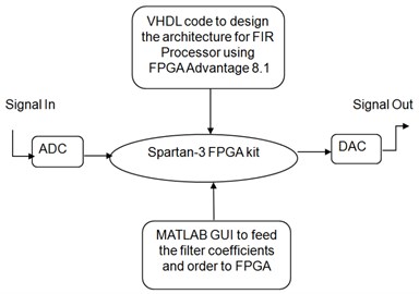
The schematic of the entire system is shown in the Fig. 1. MATLAB with graphical-user-interface (GUI) is used for inputting the filter parameters and its order as per requirement which is interfaced to the FPGA. Therefore, any filter response such as low pass, high pass, band pass or band stop for FIR can be processed. FPGA Advantage 8.1 software of Mentors has been used to design the architecture in VHDL for the specified filter processor. After successful implementation, Spartan-3 FPGA kit with ADC and DAC interface will be used for the real-time signal processing.
2. Suitable filter structure
Two most common types of digital filters: Finite Impulse Response (FIR) and Infinite Impulse Response (IIR) are generally used for the signal processing of audio frequency signals [10]. Both have different structures to process the signals. It is up to the designer to choose a suitable structure as per the requirement [11]. FIR filters are usually realized as a non-recursive (without feedback) structures. FIR recursive structures in comparison require the pole-zero cancellation. In the case of FIR filters, perfect linear phase characteristics can be achieved with flat group delay without any phase distortion and are very easy to implement with assured stability [12].
FIR filter difference equation is given as:
where, th filter coefficient, computation delay, output samples, input samples, Number of coefficients, Order of filter.
The transfer function of a filter is thus given by:
where and are the -transforms of filter input and output respectively.
In order to implement a suitable filter structure, the transfer function (H (z)) is utilized [13]. There are two structures to be considered for the implementation of FIR processor as explained in (1): Tapped Delay Line (TDL) and Time Delay & Accumulate (TDA). These structures are shown in Fig. 2. The TDL structure is selected for the implementation of FIR processor due to the following advantages: The computation is concentrated at the output. As it is just the sum of products, it is easier to implement.
Fig. 2Showing FIR filter structures: a) tapped delay line (TDL) filter, b) time delay and accumulate (TDA) filter
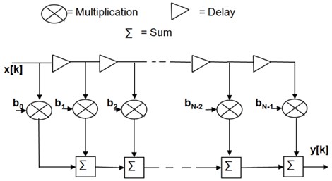
a)
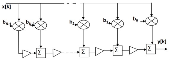
b)
3. Implementation of processor
After choosing the proposed filter structures, processor architecture, and its controller is implemented in VHDL using FPGA Advantage 8.1 software.
3.1. Data-path processor
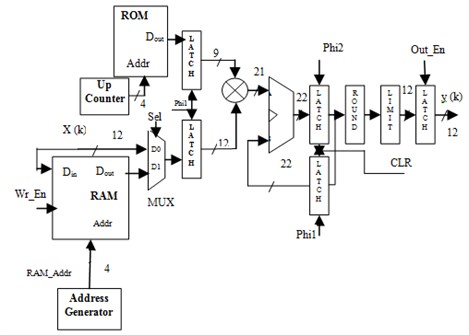
The architecture for TDL-FIR processor will be implemented using one multiplier and one accumulator and is shown in Fig. 3. The coefficients are generated in MATLAB for the desired filter specifications. The coefficients and states will be stored in the ROM and RAM respectively. There are two widths which have to be added together when the multiplication operation is performed. -bits coming from the data-path and -bits coming from the coefficients, the design accommodating for the worst-case scenario that is adding the most negative widths together and this will result in having bits coming out from the multiplier. A guard bit is needed to avoid any possible overflow, with the guard bit added, the total width will be bits. Convergent rounding is deployed to round fractional bits, applying a limiter, and the output is back to -bits word which is the same as the input. Considering the 16-tap FIR filter with the data path of 12 bits ( 12) and coefficients of 9 bits (from MATLAB) in a signed-binary fraction, the total width will be 22 bits. Convergent rounding was deployed to round eight fractional bits, thirteen bits remained at this point, applying a limiter, and the output is back to 12-bits word which is the same as the input.
Fig. 3Data-path processor
3.2. Controller design
The processor needed to be driven in a logical method, and due to the simplicity of the operation of the filter, few logic gates were able to deliver the required operations instead of using Finite State Machine (FSM). The intermediate signals which required for the operation are shown in Fig. 4. The output enable signal (Out_En) was obtained from the ROM Address bits which is the output of 4-bit up-counter as shown in Fig.4 (a). Using two AND gates would ensure that Out_En will only be enabled when ROM address reaches to “1111” (for 4-bits address length) providing that clock signal Phi2 is high.
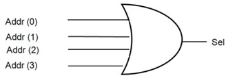
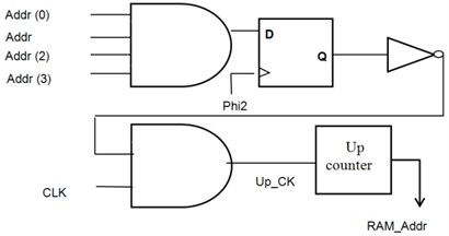
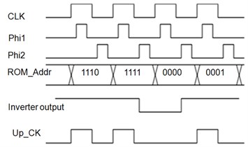
To ensure that the multiplexer uses the right value, an OR gate was used to determine the select line (Sel) as shown in Fig. 4(b). The address generator for RAM address (RAM_Addr) is shown in Fig.4(c). When the ROM’s value reached to “1111”, the output from the first AND gate turned to ‘1’ and stored in the flip-flop waiting for phi2 to be asserted high for releasing the stored value. The stored value passes through the inverter and changed into ‘0’. Having ‘0’ input to the second AND gate disabled the up-counter. An illustration of the clocking system used is shown in Fig. 5. It also shows that the Up_CK which is being suppressed in order to implement the 99-bonk clocking.
Fig. 4Control signals: a) output enable signal to enable output latch, b) select signal for multiplexer, c) address generator for RAM

a)
b)
c)
Fig. 5Clocking system used in the processor
4. Computation modelling and simulations
As described in Section 3, the model was developed in the VHDL using FPGA Advantage 8.1 commercial software. In order to describe the simulation process, a 16-tap low-pass filter with equiripple design, the sampling frequency of 45 kHz and pass-band at 8 kHz was considered. The pass-band and stop-band ripple were considered as 0.9 dB and 89 dB respectively. The data path length was selected as 12 bits from/to accommodate the 12 bit ADC/DAC. The filter coefficients were generated by MATLAB and fed to the ROM. The simulated model of the processor in VHDL is shown in Fig. 6.
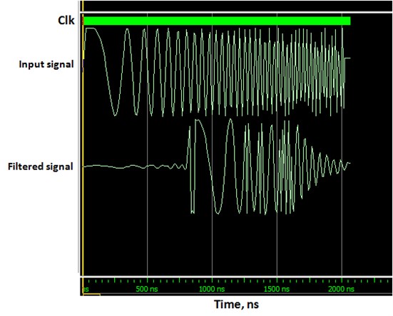
The test bench was also created in VHDL to test the model with a test stimulus of a cosine signal having normalized linear swept-frequency between 0 and 0.42. The processor model and the test bench were compiled in the ModelSim. The ModelSim is an in-built HDL simulator available in FPGA Advantage. The simulation results in Figure 7 show the low-pass filtered output with the set specifications. The design is flexible and therefore the type of filter (e.g. low-pass, high-pass, band-pass or band-stop) and its specifications can be varied as per requirement.
Fig. 6A Simulated model of FIR processor in VHDL
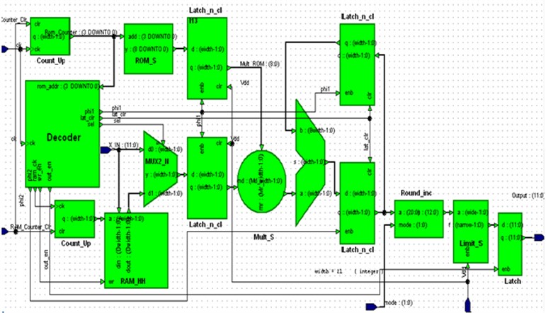
Fig. 7Simulation results of ModelSim showing the clock signal, input stimulus and the filtered output
5. Results and verification
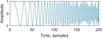
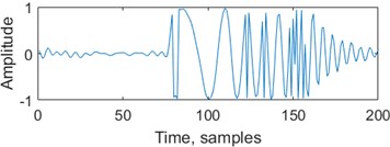
The Verifications of results were needed to determine whether the model developed model match with the set specifications. The results shown in Fig. 6 had to be compared with the MATLAB results. The same specifications of the filter and the input stimulus were used to analyze the filtered output in MATLAB. The results obtained in MATLAB are shown in Fig. 8.
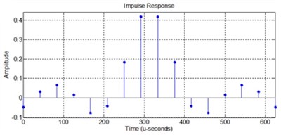
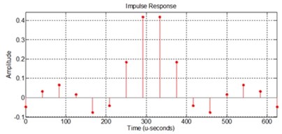
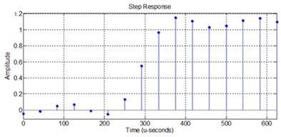
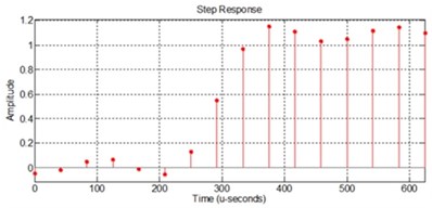
It can be clearly observed from the Fig. 7 and Fig. 8 that the results obtained in ModelSim and MATLAB are perfectly matched. In order to validate further, a 16-tap low-pass filter with equiripple design, the sampling frequency of 24 kHz, pass-band at 4.8 kHz and stop-band at 6 kHz was considered and the graphical user interface (GUI) was developed in MATLAB to generate the filter coefficients as per specifications. The impulse function and step functions were applied to both systems. The simulation result obtained from the processor-VHDL model was completely matched with the MATLAB results as shown in Fig. 9 and gives the assurance that the system was implemented correctly.
Fig. 8MATLAB results showing a) the input stimulus and b) the low-pass filtered output
a)
b)
The system can be tested for any order of FIR filter for low-pass, high-pass, band-pass or band-reject specifications. Hence, this leads to creating a flexible and universal filter for signal processing applications. It must be noted that all components of the architecture are parameterized due to the use of generic in VHDL. This leads to the same architecture be applicable for the frequency ranges other than audio frequency. The architecture can be changed depending on the algorithm for ultrasonic signal processing techniques [14-25].
Fig. 9Test results of 16-Tap FIR processor: a) impulse response in MATLAB, b) impulse response in VHDL, c) step response in MATLAB, d) step response in VHDL
a)
b)
c)
d)
6. Significance in ultrasonic signal processing
FPGA-based devices can be updated by just updating the programming and data streams and it does not require changing the hardware. It enables the FPGA to create a system-on-chip environment for testing and processing the signals and develop a highly efficient and flexible system for various applications including audio, video, and ultrasonic signal processing. Ultrasonic nondestructive testing and evaluation (UNDT&E) have been extensively and effectively used for the analysis of various components in manufacturing, such as to find the defects in composite materials. In the ultrasonic nondestructive testing (NDT), the detected echoes are random in nature with random in nature and there is a lot of noise and interference. Hence, it becomes challenging to use the backscattered echoes to extract the desired information about the defects, required for structural health monitoring. Various signal processing algorithms have been developed to characterize the non-stationary and nonlinear behavior of ultrasonic signals for NDE Applications [14].
The basic principle of FPGA-based ultrasonic signal processing is similar to the one shown in Fig. 1. ADC and DAC are required to acquire and process out the signals respectively. The signal processing algorithm required for the ultrasonic signals should be updated on embedded FPGA. There are various signal processing algorithms available for filtering and de-noising the ultrasonic signals such as cross-correlation, Hilbert Transform, autoregressive analysis, wavelet transform and split-spectrum processing (SSP) etc. [15-18]. The SSP algorithm for target detection was successfully implemented on Virtex-5 FPGA due to its capability to easier interfacing with ultrasonic equipment [19]. The algorithm can be implemented using C, MATLAB etc. and controllers can be designed in VHDL. The SSP algorithm based on C language was evaluated on FPGA platform [20-22].
The Fast Fourier Transform has a vital role in the ultrasonic testing of materials. FFT is applicable to get clear ultrasonic images, analysis of phase-velocity dispersion curves in anisotropic plates and reduction of noises. The FPGA-based architecture for 2-D FFTs was implemented for the real-time image filtering [23].
The wavelet transform (WT) is useful ultrasonic signal processing method to improve flaw detection in noisy environments and defects detection in grainy materials. The analysis of signals is also faster than Fourier transform. The wavelets are localized in both time and frequency as compared to localized in only frequency in Fourier transform. The implementation of discrete wavelet transform (DWT) using the low pass and high pass FIR filters was done with Virtex-5 FPGA device [24]. Although the entire system has been developed with 8 multipliers but with the slight changes in the algorithm, it can be implemented using a single multiplier as shown in Fig. 3. Hilbert Transform (HT) can also be implemented using FFT. The architecture for HT algorithm based on FFT was implemented on Xilinx Kintex-7 which supports 8192 points transform length using 24-bit fixed point arithmetic [25].
All architectures were developed for specific type of signal processing for ultrasonic signals. However, the proper utilization of parameterized components and improved signal processing algorithm can facilitate to develop a single architecture to switch among various ultrasonic signal processing techniques i.e. SSP, FFT, WT, HT etc. The system-on-chip can be produced for the mixed signal processing to improve the signal to noise ratio in the ultrasonic testing of composite structures [26].
7. Conclusions
This work demonstrated the design and implementation of an FIR processor for the various signal processing applications. The architecture of the processor was implemented in VHDL at register transfer level (RTL) and the obtained results were verified with MATLAB in accordance with the specifications of a filter. The implementation took into account the effects of quantization and limiting circuits to the performance of the design. The designed model was built using a single multiplier and accumulator which itself shows the efficient design. The control signals were generated using the simple combinational circuits rather than the complex state diagrams. The effective utilization of 99 bonk clocking was also the key factor. The model is flexible and can be operated for various FIR filters with different specifications. The use of a single multiplier and flexible design could reduce the overall cost and chip area which in turn facilitates the model to be used for the real-time applications such as audio signal processing.
The architecture was developed using generic in VHDL which makes it frequency-independent due to parameterized components and hence can be used for ultrasonic frequencies as well. The applicability of FPGA in the field of ultrasonic signal processing has also been reviewed and it can be concluded that various signal processing techniques in ultrasonic testing and analysis can be implemented in an effective and flexible way by making a suitable architecture in VHDL. The FPGA platform in comparison to the conventional DSP processor facilitates the parallel signal processing due to the availability of large number of hardware features. Hence a single chip can be significantly utilized for the all possible ultrasonic signal processing techniques. Moreover, high computational performance, low cost, low power requirements as compared to DSP processors and CPU based systems promotes the FPGA based processors as a better choice for the complex signal processing applications. Keeping this motivation, the presented work can be further extended to the flexible ultrasonic signal processing and noise reduction with band splitting. In the field of ultrasonic signal processing, FPGA will be a dominant platform and more robust and effective architectures can be developed in near future. As the different architectures can be switched as per requirement, it is expected to have a single architecture with some modifications for various ultrasonic signal processing techniques.
References
-
Villasenor J., Hutchings B. The flexibility of configurable computing. IEEE Signal Processing Magazine, Vol. 15, Issue 5, 1998, p. 67-84.
-
Tessier R., Burleson W. Reconfigurable computing for digital signal processing: a survey. Journal of VLSI Signal Processing, Vol. 28, 2001, p. 7-27.
-
Parvez H., Marrakchi Z., Kilic A., Mehrez H. Application-specific FPGA using heterogeneous logic blocks. ACM Transactions on Reconfigurable Technology and Systems, Vol. 4, Issue 3, 2011, p. 1-14.
-
Seals R. C., Whapshott G. F. Field programmable gate arrays (FPGAs). Programmable Logic: PLDs and FPGAs, 2011, p. 102-139.
-
Qing L., Kai C., Ying Yong L. FPGA software architecture for software defined radio. Procedia Engineering, Vol. 29, 2012, p. 2133-2139.
-
Sano K. FPGA-based systolic computational-memory array for scalable stencil computations. High-Performance Computing Using FPGAs, 2013, p. 279-303.
-
Vishnu G., Karthik P., Jabeen F. VLSI design and implementation of efficient software defined radio using Optimized Quadrature direct digital frequency synthesizer on FPGA. Procedia Computer Science, Vol. 58, 2015, p. 414-421.
-
Aboutabikh D. K., Idris D. M. B., Haidar D. I. Design and implementation of a digital accumulator for the phase coherent radio pulse signal using FPGA. International Journal of Advanced Research in Computer and Communication Engineering, Vol. 4, Issue 8, 2015, p. 493-496.
-
Mentor Graphics Corporation All rights reserved. Start here guide for FPGA Advantage, 2008. http://hornad.fei.tuke.sk/predmety/ncs/FPGA_Advantage_Documentation/hds_user.pdf.
-
Tian J., Li G., Li Q. Hardware-efficient parallel structures for linear-phase FIR digital filter. Proceedings of 56th IEEE international Midwest Symposium on Circuits and Systems, 2013, p. 995-998.
-
Winder S. Digital Fir Filter Design. Analog and Digital Filter Design, 2002, p. 377-394.
-
Proakis J. G., Manolakis D. G. Digital Signal Processing-Principles, Algorithms and Applications. Prentice-Hall, New Delhi, 2000.
-
Xu C., Yin S., Qin Y., Zou H. A novel hardware efficient FIR filter for wireless sensor networks. Proceedings of 5th IEEE International Conference on Ubiquitous and Future Networks, 2013, p. 197-201.
-
Tiwari K. A., Raisutis R. Comparative analysis of non-contact ultrasonic methods for defect estimation of composites in remote areas. CBU International Conference Proceedings, Vol. 4, 2016, p. 846-851.
-
Abbate A., Koay J., Frankel J., Schroeder S. C., Das P. Signal detection and noise suppression using a wavelet transform signal processor: Application to ultrasonic flaw detection. IEEE Transactions on Ultrasonics, Ferroelectrics and Frequency Control, Vol. 44, Issue 1, 1997, p. 14-26.
-
Shankar P. M., Karpur P., Newhouse V. L., Rose J. L. Split-spectrum processing: Analysis of polarity threshold algorithm for improvement of signal-to-noise ratio and detectability in ultrasonic signals. IEEE Transactions on Ultrasonics, Ferroelectrics and Frequency Control, Vol. 36, Issue 1, 1989, p. 101-108.
-
Mallett R., Mudge P. J., Gan T. H., Balachandra W. Analysis of cross-correlation and wavelet de-noising for the reduction of the effects of dispersion in long-range ultrasonic testing. Insight - Non-Destructive Testing and Condition Monitoring, Vol. 49, Issue 6, 2007, p. 350-355.
-
Bouden T., Dib S., Aissaous K., Grimes M. Signal processing methods for materials defects detection. IEEE International Ultrasonics Symposium, 2009.
-
Lu Y., Ahn I. S., Smith R. FPGA-based ultrasonic signal processing platform. IEEE International Conference on Electro Information Technology (EIT), Grand Forks, ND, 2016.
-
Oruklu E., Saniie J. Hardware efficient realization of a real time ultrasonic target detection system. IEEE Transaction on Ultrasonics, Ferroelectrics, and Frequency Control, Vol. 56, Issue 6, 2009, p. 1262-1269.
-
Sun H. C., Saniie J. Ultrasonic flaw detection using split-spectrum processing combined with adaptive network based fuzzy inference system. IEEE Proceedings of Ultrasonic Symposium, Vol. 1, 1999, p. 801-804.
-
Saniie J., Oruklu E., Yoon S. System-on-chip design for ultrasonic target detection using split-spectrum processing and neural networks. IEEE Transactions on Ultrasonics, Ferroelectrics, and Frequency Control, Vol. 59, Issue 7, 2012, p. 1354-1368.
-
Uzun I. S., Amira A., Bouridane A. FPGA implementations of fast Fourier transforms for real-time signal and image processing. IEE Proceedings – Vision, Image, and Signal Processing, Vol. 152, Issue 3, 2005, p. 283-296.
-
Velukar S. S., Parlewar M. P. FPGA implementation of fir filter using distributed arithmetic architecture for DWT. International Journal of Computer Applications, Vol. 92, Issue 16, 2014, p. 12-16.
-
Prince A., Verma P. K., Jayakumar Raju C. D. Efficient architecture for real time implementation of Hilbert Transform in FPGA. IEEE International Conference on Electrical, Computer and Communication Technologies (ICECCT), 2015, p. 1-5.
-
Tiwari K. A., Raisutis R., Samaitis V. Signal processing methods to improve the Signal-to-noise ratio (SNR) in ultrasonic non-destructive testing of wind turbine blade. Procedia Structural Integrity, Vol. 5, 2017, p. 1184-1191.
About this article
This research work was supported by the Multimedia Engineering Department and Ultrasound Research Institute, Kaunas University of Technology, Lithuania.
