Abstract
The proposed research involves the design and implementation of a novel hybrid Topology for Power Quality Improvement using Multilevel Inverter to reduce vibration and noise in BLDC motor for industrial applications. The utility of power electronics device plays a vital role for various applications in recent days. Similarly, the power consumption is also important for all processing units. The power electronic devices contain a lot of converters for processing the energy. During such cases, the harmonics are produced in different ways. Hence, a system analysis is necessary to find the problem at conventional methods. Hence the problem is identified on the distribution static compensator (DSTATCOM) component module whose harmonics are high, and it is important module for the circuit, hence preventive action to be taken to reduce the harmonics. To limit or reduce the harmonics, it is required to modify the triggering mechanism and control unit of Multi level inverter. Hence, the proposed hybrid method is implemented with the developed H-bridge and diode clamped topology with a brushless dc motor. In addition, the vibrations and the noise level are also reduced due to the reduced total harmonic distortion. The proposed module is simulated on MATLAB Simulink, and an experimental analysis is carried out to verify functionality tools with various operating conditions, the proposed method proves more efficient than the switches and complex networks present in traditional methods.
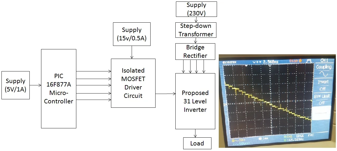
Highlights
- CMLI creates the stepped alternating current pulses with additional DC power with compact oscillations content.
- The input DC voltage is highly energized toward desired potential level through BB Cuk converter system.
- The improved PSO algorithm is used to optimize the parameters of least squares support vector machines (LS-SVM).
- Constructing an optimal LS-SVM classifier are used to classify the fault.
- A novel signal processing method called Empirical Wavelet Transform (EWT) is used to decompose vibration signal.
- The level of the harmonics and its supply power were analyzed and reduced.
1. Introduction
With the advancing deregulation of the electric utility industry, different changes are always recognized. Since, the power is continuously considered as a thing, transmission systems are pushed closer to their quality and warm purposes of limitation, while the accentuation on the idea of vitality became huger than in another time. In the deregulated utility condition, money-related and promotion powers will continue to ask for a more perfect and productive task of the power framework regarding age, transmission, and circulation. Presently, like never before, cutting edge advancements are foremost for the strong and secure task of energy systems. Power electronic based equipment such as Flexible AC Transmission Systems (FACTS), High-Voltage DC (HVDC), and Custom Power advancements constitute a segment of the most encouraging particular movements to address the new working challenges being displayed today. These degrees of progress rely upon a better limit of vitality electronic apparatus in order to quickly react to framework occasions. So, the increment control exchange restricts and enhances the nature of energy conveyed. In the past couple of years, the high-power applications are leading the world with the respect of their wide expanding consideration. Since, numerous topologies, strategies and drive applications are reviewed and discussed. Such converters are reasonable with high power devices based on their rating. Reference [1, 2] framed the multilevel power conversion topology with neutral point clamped topology. Recent days, the demand in electronics devices was associated with many fast charging devices which external energy sources require early investigation on harmonic and non-active power compensation [3, 4]. This widespread harmonic polluting device both reduces the system efficiency and has detrimental impacts on grid voltage distortion levels [5]. Hence, the addition of current leads to heat losses and creates some issues in sensitive electrical devices. Some recent researchers are focused on power quality issues and current harmonics. Power Quality is the way to effective conveyance of quality item and the activity of an industry. It is presently significantly more basic for the business on account of expanding use of electronic loads and electronic controllers which are complex to the nature of energy provided. The expanding emphasis on the general power framework effectiveness brought about the utilization of devices such as high effectiveness, flexible speed engine drives and shunt capacitors for control factor remedy to decrease losses bringing about expanding consonant levels on control frameworks. For various applications like agricultural and industrial different topologies of power-controlled devices are designed to embed with the renewable resources. Henceforth Multilevel inverters (MLIs) are growing as a current scientific thing of power-controlled devices for high-power applications [6]. Power-controlled devices clamped multilevel inverter (PMLI), soaring capacitor MLI (SCMLI) and multilevel inverter which is cascaded (CMLI) are the three major parameters of MLI [7]. CMLI creates the stepped alternating current pulses with additional DC power with compact oscillations content [8]. It acts as an extra gorgeous topology compared to other two topology. Conventional Cascaded Multilevel inverter (CCMLI) is shown in Fig. 1.
The structure is reconstructed with three renewable sources with a permanent magnet brushless DC motor. Cascaded Multilevel inverter with BLDC motor (CMLIBLDC) is shown in Fig. 2.
Fig. 1Schematic circuit diagram of CCMLI
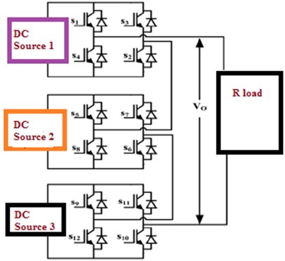
Fig. 2Schematic circuit diagram of (CMLIBLDC)
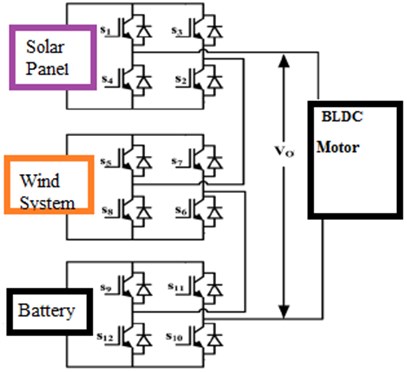
For obtaining output nominal in CCMLI, new topology, such as multilevel converter topology is proposed between the various input sources moreover considering transformer. An effective use of CCMLI, buck-boost Cuk cascaded multilevel inverter (BBCCMLI) topology modifications is despoiled due to the lot of power controlled devices and Direct current power. The proposed cascaded DC link circuit diagram is shown in Fig. 3.
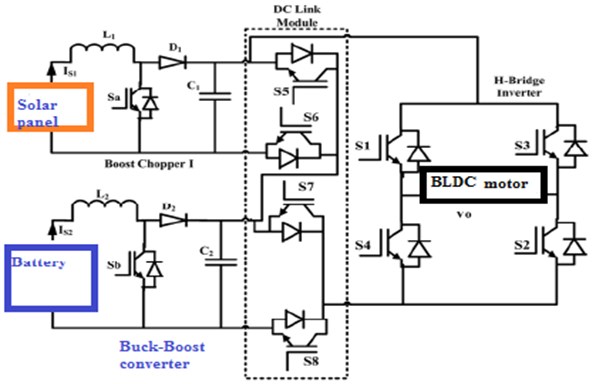
Meanwhile topological alterations are made in the existing CCMLI [9-13]. Henceforth in proposed research, the two buck-boost converter circuit is introduced between input sources and DC-link inverter to obtain nominal output voltage. The input DC voltage is highly energized toward desired potential level through BB Cuk converter system. Such modifications of topology results in the reduction of power controlled devices and input sources. For this research, a single-phase thirty-one-stage asymmetrical power DC-DC Cuk linking direct current cascaded multilevel CMLI (BBCDCLCMLI) network is designed for industrial and agricultural Usages. Schematic circuit of the designed BBCDCLCMLI structure is given on Fig. 4.
Fig. 3Proposed schematic diagram of DC-DC Cascaded DC-link Multilevel inverter
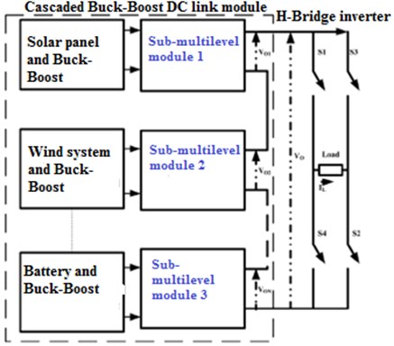
Fig. 4Proposed circuit diagram of BBCDCLCMLI with BLDC motor
Achieving improved superiority of AC power (by reducing oscillations on converter), to get sinusoidal wave a multicarrier pulse width modulation is proposed accordingly power-controlled device topology is intended to linking direct current controlled devices [14-17]. The improved PSO algorithm is used to optimize the parameters of least squares support vector machines (LS-SVM) in order to construct an optimal LS-SVM classifier, which is used to classify the fault. Finally, the proposed fault diagnosis method is fully evaluated by experiments and comparative studies for motor bearing for reduction of vibration [18]. Another algorithm MGACACO is proposed makes use of the exploration capability of GA and stochastic capability of ACO algorithm. In the proposed MGACACO algorithm, the multi-population strategy is used to realize the information exchange and cooperation among the various populations. The chaotic optimization method is used to overcome long search time, avoid falling into the local extremum and improve the search accuracy [19]. A vibration signal analysis method is the most popular technique that is used to monitor and diagnose the fault of motor bearing. However, the application of the vibration signal analysis method for motor bearing is very limited in engineering practice. In this paper, on the basis of comparing fault feature extraction by using empirical wavelet transform (EWT) and Hilbert transform with the theoretical calculation, a new motor bearing fault diagnosis method based on integrating EWT, fuzzy entropy, and support vector machine (SVM) called EWTFSFD is proposed. In the proposed method, a novel signal processing method called EWT is used to decompose vibration signal into multiple components in order to extract a series of amplitude modulated-frequency modulated (AM-FM) components with supporting Fourier spectrum under an orthogonal basis is proposed [20]. The vibration signal of motors under no-load and load states are used to testify the effectiveness of the proposed HMGSEDI method. The experiment shows that high-order differential mathematical morphology entropy can more effectively identify the fault damage degree of bearings and the identification accuracy of fault damage degree can be greatly improved. Therefore, the HMGSEDI method is an effective quantitative fault damage degree identification method and provides a new way to identify fault damage degree and fault prediction of rotating machinery are proposed [21]. The new algorithm is proposed on the reduction of vibration on motor [22]. Another approach, the Alpha-stable distribution theory is used to replace the uniform distribution in order to escape from the local minima in a certain probability and improve the global search ability. Next, the DOADAPO algorithm is used to solve the constructed multi-objective optimization model of gate assignment in order to fast and effectively assign the gates to different flights in different time [23].
2. Materials and methods
BBCDCLMLI contains dual unbalanced Direct current power, DC-DC Cuk converter unit, linking voltage DC and hybrid topology. Hybrid topologies are connected parallel on dc-link network.
2.1. DC-link configuration on improved converter
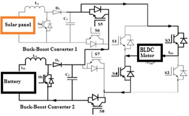
BBC converter element are connected in unbalanced power sources, additionally DCLM has dual MOSFET switch whose output is always in one direction. Fig. 4 shows the Corresponding schematic circuit of BDCLMLI.
BDCLMLI configuration is calculated by number of levels:
BDCLCMLI proposed the quantity of switches are given by Eq. (2):
where is the number of levels, gives the quantity details of power switches used in BBCDCLMLI, – denotes the hybrid topology inverter, – denotes the required amount of DC power and – denotes the quality of DC-DC Cuk units.
2.2. Modes of operation
2.2.1. Approach denotes the BBC DC-link topology
For obtaining thirty-one-stage Alternating Current output using dual unbalanced power units, Designed structure will operate in four approaches.
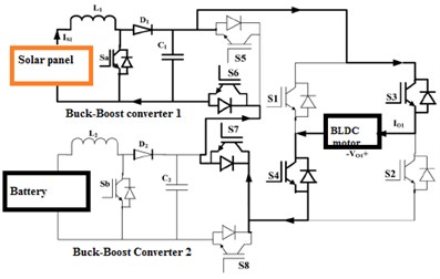
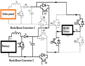
• Operation modes A and B: In the operation modes 1 and 2, the source voltage is boosted to by activating the BBC switch and the DC-link switches are and . The corresponding circuits for these modes are shown in Fig. 5(a) and (b).
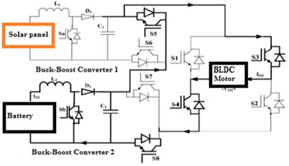
Fig. 5Proposed model of operation modes: a) approach A, b) approach B, c) approach C, d) approach D
a)
b)
c)
d)
When , the BBC converter device energized correspondingly inductor current linearly increases towards -.
Inductor voltage are given as:
Energy to the inductor using source are obtained by:
hence , BBC switch energizes, inductor L1 current decreases linearly at -.
Output voltage of converter 1 obtained using Eq. (5):
Inductor releases the energy which is fed to DCLM are obtained by Eq. (6):
Average output voltage of DC-DC converter 1 with lossless are obtained by Eq. (7):
Voltage variation across the capacitor can be expressed by Eq. (8):
where is the DC input voltage 1, determines the current source 1, K1 denotes the duty ratio of DC-DC converter 1, is the load output of buck boost converter 1.
• Operation modes C and D: In operation modes E and H, the input voltages and are Stepped up to and by energizing the buck boost converter devices and . Switches and conducts.
When , the buck boost converter switches and are energized, and the current through the inductors and increases linearly from to and from to , respectively.
At , enhanced converter and switches are de-energized accordingly inductor current and deenergizes linearly from - and from -, correspondingly:
Inductor gets the energy fed via source obtained using Eq. (10):
hence , the BBC device are deenergized, inductor current decreases linearly from -.
Hence the voltage across converter 2 given by using Eq. (11):
Inductor releases energy which is fed DCLM are obtained by Eq. (12):
Average output voltage of DC-DC converter 2 with lossless are obtained by Eq. (13):
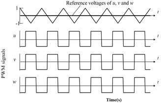
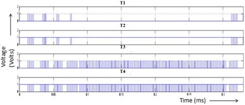
A model of single-phase BBCDCLCMLI-based motor for 195V () output voltage was designed. Fig. 6(a), (b) represents Carrier signals, PWM pulses using n-levels. Experimental hardware has rectifier units, buck boost converter units, controller units, driver units, DC-link and H-bridge inverter units. Capacitive filter of 1000 μF, bridge rectifier (MICBR1010) are used for designing rectifier unit. The input converter units and battery banks are fed from the outputs of rectifier units. The buck boost converter (1 and 2) are fabricated using IRF840 controlled power devices (MOSFET) switches and passive components ( 2 mH and 100 μF). MOSFET driver circuit gets control signals from dspic units. The features of dspic are used to achieve successful control of the proposed system. The proposed experimental diagram BBCDCLCMLI system is shown in Fig. 5(c). Table 1 shows the power-controlled devices turning states at various levels.
Capacitor voltage change is obtained by Eq. (14):
where is the DC input voltage 2, determines the current source 2, denotes the duty ratio of DC-DC converter 2, is the load output of buck boost converter 2.
• Operation modes E and H: In operation modes E and H, the input voltages and are Stepped up to and by energizing the buck boost converter devices and . Switches and conducts.
Table 1Power controlled devices turning state of BBCDCLMLI
Potential rating, Volts | States level | Switch turning levels | ||||||||
30 | 1 | 0 | 1 | 1 | 1 | 0 | 0 | 0 | 1 | 1 |
35 | 2 | 1 | 0 | 1 | 1 | 0 | 0 | 1 | 0 | 0 |
40 | 3 | 0 | 1 | 1 | 1 | 0 | 0 | 0 | 1 | 0 |
45 | 4 | 1 | 1 | 0 | 0 | 0 | 0 | 0 | 0 | 0 |
50 | 5 | 0 | 1 | 0 | 0 | 1 | 1 | 0 | 1 | 1 |
55 | 6 | 1 | 0 | 0 | 0 | 1 | 1 | 1 | 0 | 0 |
60 | 7 | 0 | 0 | 0 | 0 | 1 | 1 | 0 | 1 | 0 |
65 | 8 | 0 | 0 | 0 | 0 | 1 | 1 | 0 | 1 | 0 |
70 | 9 | 0 | 1 | 1 | 1 | 0 | 0 | 0 | 1 | 1 |
75 | 10 | 1 | 0 | 1 | 1 | 0 | 0 | 1 | 0 | 0 |
80 | 11 | 0 | 1 | 1 | 1 | 0 | 0 | 0 | 1 | 0 |
85 | 12 | 1 | 1 | 0 | 0 | 0 | 0 | 0 | 0 | 0 |
90 | 13 | 0 | 1 | 0 | 0 | 1 | 1 | 0 | 1 | 1 |
95 | 14 | 1 | 0 | 0 | 0 | 1 | 1 | 1 | 0 | 0 |
100 | 15 | 0 | 0 | 0 | 0 | 1 | 1 | 0 | 1 | 0 |
105 | 16 | 0 | 0 | 0 | 0 | 1 | 1 | 0 | 1 | 0 |
110 | 17 | 0 | 1 | 1 | 1 | 0 | 0 | 0 | 1 | 1 |
115 | 18 | 1 | 0 | 1 | 1 | 0 | 0 | 1 | 0 | 0 |
120 | 19 | 0 | 1 | 1 | 1 | 0 | 0 | 0 | 1 | 0 |
125 | 20 | 1 | 1 | 0 | 0 | 0 | 0 | 0 | 0 | 0 |
130 | 21 | 0 | 1 | 0 | 0 | 1 | 1 | 0 | 1 | 1 |
135 | 22 | 1 | 0 | 0 | 0 | 1 | 1 | 1 | 0 | 0 |
140 | 23 | 0 | 0 | 0 | 0 | 1 | 1 | 0 | 1 | 0 |
145 | – | 0 | 0 | 0 | 0 | 1 | 1 | 0 | 1 | 0 |
140 | 24 | 0 | 1 | 1 | 1 | 0 | 0 | 0 | 1 | 1 |
155 | 25 | 1 | 0 | 1 | 1 | 0 | 0 | 1 | 0 | 0 |
160 | 26 | 0 | 1 | 1 | 1 | 0 | 0 | 0 | 1 | 0 |
165 | 27 | 1 | 1 | 0 | 0 | 0 | 0 | 0 | 0 | 0 |
170 | 28 | 0 | 1 | 0 | 0 | 1 | 1 | 0 | 1 | 1 |
175 | 29 | 1 | 0 | 0 | 0 | 1 | 1 | 1 | 0 | 0 |
180 | 30 | 0 | 0 | 0 | 0 | 1 | 1 | 0 | 1 | 0 |
195 | 31 | 0 | 0 | 0 | 0 | 1 | 1 | 0 | 1 | 0 |
When , the buck boost converter switches and are energized, and the current through the inductors and increases linearly from to and from to , respectively.
At this instant, the energy input to the inductor from the source and the energy input to the inductor from the source are expressed using Eq. (15):
At , enhanced converter and switches are de-energized accordingly inductor current and deenergizes linearly from - and from -, correspondingly.
Hence situation, released inductors energy and of DCLM is determined as:
Fig. 6a) Carrier signal, b) PWM pulses for proposed system
a)
b)
2.2.2. Hybrid topology inverter bridge configuration operation
The cascaded multilevel inverter is made out of various single-stage H-bridge inverters and is ordered into symmetric and asymmetric groups in light of the size of dc voltage sources. In the symmetric kinds, the sizes of the dc voltage sources of all H-spans are equivalent while in the asymmetric sorts, the estimations of the dc voltage wellsprings of all H-spans are extraordinary. At present, a few topologies with different control strategies have been introduced for cascaded multilevel inverters. This research considered this H bridge concept and implemented in this system. The above topology inverter unit operates in dual operation. Alternating current at positive voltage are obtained with the use of Eqs. (17)-(19):
At approach (b), the alternating current output voltage at negative cycle are synthesized and energized by Hybrid power devices and are given in Figs. 5(b) and (d).
Alternating current at negative voltage are obtained by:
2.2.3. Buck boost converter conduction losses
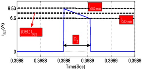
MOSFET switching losses are calculated using the accurate voltage drop with series linear resistor 0.07. It determines the terminal gate by terminal source voltage and junction temperature. The losses in the MOSFET switch are given in Eq. (23):
where indicates the current flowing through the switch , stands for the “ON” time of switch and delta stands for the average ripple current of switch. Switching ampere determined as is derived from Eq. (23):
Harmonics current are given as in Eq. (24):
where and gives high and low magnitudes of power-controlled device current - as illustrated in Fig. 7. From Fig. 6, 0.22, 7.565 and 0.965, which are substituted in Eq. (24), sum amperes and losses are derived from MOSFET switches as resolved in Eq. (25):
Fig. 7MOSFET switches conduction waveform at open-loop condition
2.2.3.1. Switching conduction losses during starting
Buck boost Cuk converter diode losses.
Converters diode losses due to forward voltage 0.8 V are expressed by Eq. (26):
where is ampere via diode, represents “ON” time of diode, hence the harmonic amps are obtained from Eq. (27):
where , represents the high and low magnitudes of diode, which is shown in Fig. 8. Fig. 8 shows 0.15, 0 and 3.25 and total torque ripple voltage across each components. The values are substituted in Eq. (27), the total current conduction and the power loss of diode, as resolved in Eq. (28):
2.2.3.2. Converters inductor losses and
The open-loop waveforms of converter inductor are shown in Fig. 8. Meanwhile, inductor losses and have two factors. First factor is wire loss or core loss. It is given by Eq. (29) for a wire:
Therefore, the mean harmonic current is given in Eq. (30):
Fig. 8Converter: a) diode losses, b) ripple voltages across components [24]
![Converter: a) diode losses, b) ripple voltages across components [24]](https://static-01.extrica.com/articles/20306/20306-img12.jpg)
![Converter: a) diode losses, b) ripple voltages across components [24]](https://static-01.extrica.com/articles/20306/20306-img13.jpg)
3. Results and discussions
3.1. Simulation performance evaluation
The proposed control topology is tried with a perfect three-stage connection with a two-phase BBC power supply and a permanent magnet synchronous motor load. Simulation Specifications are shown in Table 2.
Table 2Simulation specifications for converter
S. No | Objects | Values |
1 | Maximum PV module voltage | 24 V |
2 | Maximum PV module current | 1.04 A |
3 | Maximum PV module power | 74 W |
4 | TPC output voltage | 48 V |
5 | TPC output power | 40 W |
6 | Rated BLDC motor power (Torque = 0.125 Nm, Speed = 2000 Rpm, DC link voltage = 24 V, number of poles = 8) | 39 W |
7 | Nominal power of battery (Nominal voltage = 12 V, Nominal current = 7 A/h) | 84 W/h |
To verify the asymmetrical performance of converters, an input DC voltage source is considered to be 18 V as shown in Fig. 9. Further, load resistances 28.8 Ω are considered for a symmetrical condition. The output voltages of the MOBB converter are desired to be regulated on 30 V and 18 V from 0 to 0.4 Sec. At a particular time, i.e. from 0.4 Sec to 0.8 Sec, the MOBB converter output voltages are desired to be regulated on 18 V and 30 V respectively. In Figs. 9(b) and (c), output voltages and are shown. As seen from this figure, the output voltages are tracked by the reference values and with a minimum steady state error. It is obvious that the output voltages are regulated very well. Similarly, the currents and are drawn from load resistances and as shown in Fig. 9(d) and (e). At this time, load resistances 31.25 W and 11.25 W consume power from the input supply till 0.4 sec, consequently after 0.4 sec load, resistances consume power from the input supply 11.15 W and 31.25 W respectively. Therefore powers and are drawn under asymmetrical output voltage condition as shown in Fig. 9(f) and (g). In Fig. 9(h), the total output voltage and total output power are represented. As seen from this figure, voltage and power are tracked by the reference values 48 V and 42.5 W. It is obvious that the output voltage and power are regulated smoothly. Fig. 9(i) and (j) shows battery, motor outputs. The converter works in three conditions by using battery BCD, PVD, BDD.
Fig. 9a)-h) Converter asymmetrical output, battery, i), j) motor parameters outputs, k) BCD, l) PVD, m) BDD [24]
![a)-h) Converter asymmetrical output, battery, i), j) motor parameters outputs, k) BCD, l) PVD, m) BDD [24]](https://static-01.extrica.com/articles/20306/20306-img14.jpg)
a)
![a)-h) Converter asymmetrical output, battery, i), j) motor parameters outputs, k) BCD, l) PVD, m) BDD [24]](https://static-01.extrica.com/articles/20306/20306-img15.jpg)
b)
![a)-h) Converter asymmetrical output, battery, i), j) motor parameters outputs, k) BCD, l) PVD, m) BDD [24]](https://static-01.extrica.com/articles/20306/20306-img16.jpg)
c)
![a)-h) Converter asymmetrical output, battery, i), j) motor parameters outputs, k) BCD, l) PVD, m) BDD [24]](https://static-01.extrica.com/articles/20306/20306-img17.jpg)
d)
![a)-h) Converter asymmetrical output, battery, i), j) motor parameters outputs, k) BCD, l) PVD, m) BDD [24]](https://static-01.extrica.com/articles/20306/20306-img18.jpg)
e)
![a)-h) Converter asymmetrical output, battery, i), j) motor parameters outputs, k) BCD, l) PVD, m) BDD [24]](https://static-01.extrica.com/articles/20306/20306-img19.jpg)
f)
![a)-h) Converter asymmetrical output, battery, i), j) motor parameters outputs, k) BCD, l) PVD, m) BDD [24]](https://static-01.extrica.com/articles/20306/20306-img20.jpg)
g)
![a)-h) Converter asymmetrical output, battery, i), j) motor parameters outputs, k) BCD, l) PVD, m) BDD [24]](https://static-01.extrica.com/articles/20306/20306-img21.jpg)
h)
![a)-h) Converter asymmetrical output, battery, i), j) motor parameters outputs, k) BCD, l) PVD, m) BDD [24]](https://static-01.extrica.com/articles/20306/20306-img22.jpg)
i)
![a)-h) Converter asymmetrical output, battery, i), j) motor parameters outputs, k) BCD, l) PVD, m) BDD [24]](https://static-01.extrica.com/articles/20306/20306-img23.jpg)
j)
![a)-h) Converter asymmetrical output, battery, i), j) motor parameters outputs, k) BCD, l) PVD, m) BDD [24]](https://static-01.extrica.com/articles/20306/20306-img24.jpg)
k) In this mode, PV both supplies load and delivers power to battery. This condition occurs when PV power is maximum as compared with the load power, therefore the battery must to be charged. In BCD, switches , , are active and switch is entirely OFF
![a)-h) Converter asymmetrical output, battery, i), j) motor parameters outputs, k) BCD, l) PVD, m) BDD [24]](https://static-01.extrica.com/articles/20306/20306-img25.jpg)
l) With the above approach, PV only supplies loads. This situation acts when PV power is equal to motor power. During PVD, switches , are energized, and switches and are OFF
![a)-h) Converter asymmetrical output, battery, i), j) motor parameters outputs, k) BCD, l) PVD, m) BDD [24]](https://static-01.extrica.com/articles/20306/20306-img26.jpg)
m) In the above approach, dual sources PV and battery are energized for delivering the load. In BDD, switch is OFF, and switch , , are ON
The converter outputs are fed to multilevel inverter switches. The recreation parameters are set as follows: supply frequency = 50 Hz, input voltage = 480 V, input current = 27 A, exchanging frequency = 2 kHz, resistance = 20 Ω, inductance =310 mH for 31 level inverter; using the MATLAB platform, the output voltage are synthesized. Multilevel inverters with 31-levels output voltage synthesis are shown in Fig. 10.
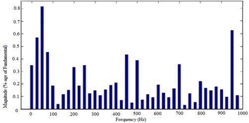
Figs. 10, 11 and 12 display steady state conditions of the simulated output voltage, current waveforms and the harmonic profile of the output voltage. To get an equation for THD, please note that the average power of the cosine at a single harmonic is given by:
where 1 represents the fundamental and ≥ 2 are the harmonics. Also note that the total average power in the signal is given by the sum of the average powers at each harmonic:
As such the THD can be calculated by finding the total power in all harmonics divided by the power in the fundamental:
In reality, there is no way to measure the infinite harmonic, so the THD measurement is usually truncated to a certain harmonic. Also note that the Fourier coefficients are required for this measurement but that the spectrum analyzer provides values in dBmV:
Because the THD is a ratio of powers, it is unit-less and is expressed as a percentage. It can also be expressed in dB as:
Fig. 10Multilevel inverter with 31-levels output voltage synthesis
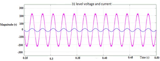
Fig. 11THD for 31 level with Developed H bridge converter module
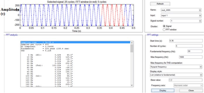
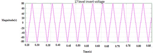
The study and analysis of the diode clamped 31-level inverter, flying capacitor-clamped 31-level inverter, cascaded 31-level inverter as well as the proposed bridged-insert cascaded 31-level inverter were carried out using MATLAB/ Simulink Tool. The voltage output obtained across the load or in other words, at the pole was analyzed and compared. Not only that, the FFT (Fast Fourier Transform) analysis was also done in order to analyze the harmonic distortion present in the output. On comparison of the results obtained, it is evident that the proposed bridged-insert cascaded MLI is much more superior to the other discussed topologies when comparing the total harmonic distortion (THD) as well as the area usage. The various levels are analyzed from 5-level, nine level twenty-five level and thirty-one level.
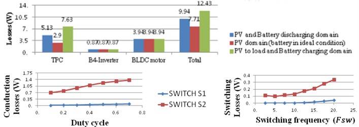
Fig. 12a) Output voltage for 17-level MLI, b) losses, duty cycle
a)
b)
Fig. 13Harmonic analysis of 17 level inverter with developed H-bridge converter
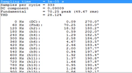
3.2. Diode clamped MLI
Fig. 14The output voltage waveform of the 5-level diode-clamped MLI
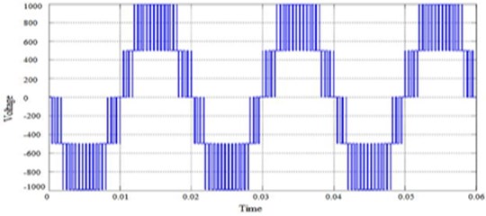
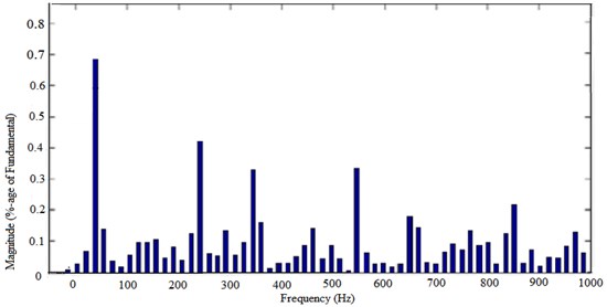
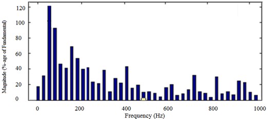
Fig. 15The FFT of the 5-level diode-clamped MLI. Fundamental (50 Hz) = 38.7 Hz, THD = 21.97 %
3.3. Flying-capacitor clamped MLI
Fig. 16The output voltage waveform of the 5-level flying capacitor clamped MLI
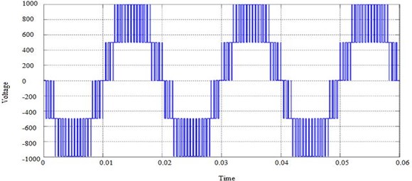
Fig. 17The FFT of the 5-level flying capacitor clamped MLI. Fundamental (50 Hz) = 967.4 Hz, THD = 39.92 %
3.4. Conventional cascaded MLI
Fig. 18The output voltage waveform of the 5-level cascaded MLI
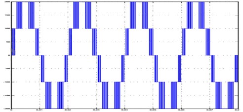
Fig. 19The FFT of the 5-level cascaded MLI. Fundamental (50 Hz) =278.6 Hz, THD = 20.93 %
3.5. Novel bridged-insert cascaded MLI
Fig. 20The output voltage waveform of the 5-level bridged-insert cascaded MLI
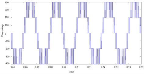
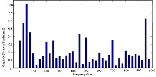
Fig. 21The FFT of the 31-level bridged-insert cascaded MLI. Fundamental (50 Hz) = 120 Hz, THD = 18.93 %
3.6. Analysis and comparison
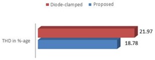
The results from section V have been consolidated in this section using bar-chart. Figs. 22, 23 show the comparison of the proposed bridged-insert cascaded MLI with diode-clamped, flying capacitor clamped and conventional cascaded MLI topologies in terms of the fundamental frequency, area coverage and THD as given in Table 3.
Table 3Result summary
Type | Fundamental in Hz | THD in %-age | Area (number of transistors) |
Diode-clamped | 38.7 | 21.97 | 8 |
Flying-capacitor clamped | 967.4 | 39.92 | 8 |
Conventional cascaded | 278.6 | 20.93 | 8 |
Proposed | 120 | 18.78 | 4 |
Fig. 22Fundamental frequency comparison: diode-clamped MLI vs proposed

Fig. 23THD comparison: diode-clamped MLI vs proposed
The Table 4 shows the various level comparisons.
Table 4THD comparison of diode clamped and developed H-Bridge based 17 and 31 level MLI topology
Parameter | Proposed | |
Diode clamped | Developed H bridge | |
THD for level 31 (%) | 12.5 | 2.17 |
THD for level 9 (%) | 46.11 | 4.77 |
THD for level 17 (%) | 32.11 | 4.39 |
THD for level 24 (%) | 22.09 | 4.30 |
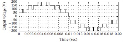
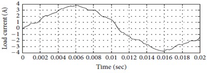
Fig. 24Simulation result for nine-level cascaded circuit of multilevel inverter
a) Output voltage
b) Load current
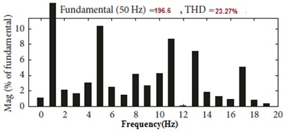
c) Harmonic contents of output voltage
Fig. 25Simulation result for twenty five-level cascaded circuit of multilevel inverter
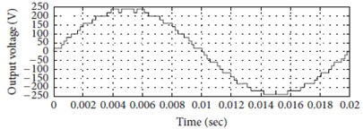
a) Output voltage
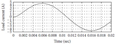
b) Load current
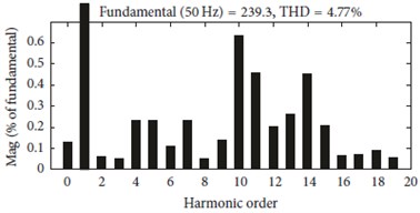
c) Harmonic contents of output voltage
Fig. 26Simulation result for thirty one-level cascaded circuit of multilevel inverter
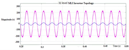
a) Output voltage
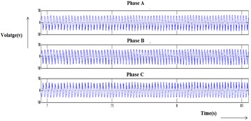
b) Load current
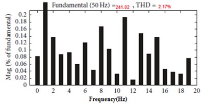
c) Harmonic contents of output voltage
3.7. Experimental evaluation
The converter outputs are fed to multilevel inverter switches. The recreation parameters are set as follows: supply frequency = 50 Hz, input voltage = 480 V, input current = 27 A, exchanging frequency = 2 kHz, resistance = 20 Ω, inductance =310 mH for 31 level inverter. Table 5 indicates motor parameters.
Fig. 27Experimental circuit diagram of BBCDCLMLI
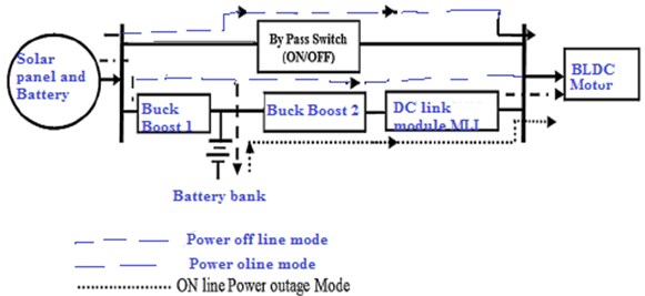
Fig. 28Realization of hardware circuit diagram of BBCDCLMLI
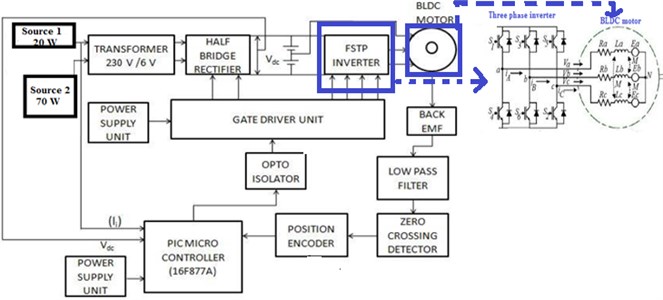
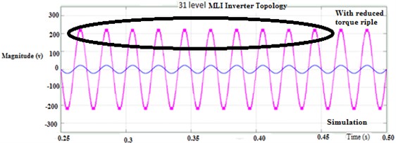
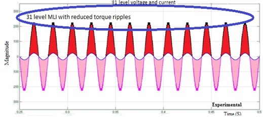
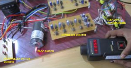
The experimental circuit diagram and realization of hardware model are shown in Figs. 27 and 28. The corresponding effective results are carried as shown in Fig. 29. Prototype hardware circuit diagrams of BBCDCLMLI are shown in Fig. 30. Comparisons were carried out with various level inverters and proved with reduced torque ripple and vibrations, and noise was reduced with the proposed system.
Table 5Motor parameters specifications
S.NO | Name of the equipment | Range |
1 | Battery | 12 V/4.7 AH |
2 | Step down transformer | 230 V/12 V |
3 | Step down transformer | 230 V/5 V |
4 | MOSFET | IRFZ24N 17 A, 55 V, 0.07 ohm, N-CHANNEL, Si, POWER, MOSFET, 220 AB |
5 | BLDC motor | 220 V, 100 A, 60 rpm |
Fig. 29Thirty-one-level MLI: a) simulation output, b) experimental output
a)
b)
Fig. 30Prototype hardware circuit diagram of BBCDCLMLI sensing speed
3.7.1. Reduction of mechanical vibration on motor and comparative analysis of total harmonic distortion
The major drawbacks of BLDC motor consist in torque ripple that causes mechanical vibrations and acoustic noise. In industry engineering of electric hybrid vehicles, the torque ripple could result in mechanical vibration and acoustic noise. Thus, it is undesirable for most of the applications. In this research the Total Harmonic Distortion in the voltage and current waveform, RMS level of vibration, and noise has been examined, and their comparison is shown in table. The RMS level of the vibration is calculated using the Matlab software. The hardware prototype model was developed for BBCDCCLMI, torque ripples are calculated using a vibration sensor, and vibrations are calculated as shown in Fig. 31. This proves that the proposed BBCDCMMLI method is able to suppress the torque ripple and mechanical vibration, and its prototypes are shown in Fig. 32. Table 6 shows the comparison of various parameters for the measurement of vibration proposed is more efficient than the conventional.
Fig. 31Realization of hardware circuit diagram of BBCDCLMLI for sensing vibration
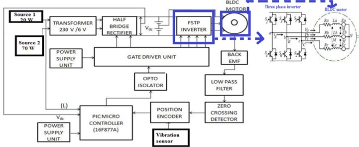
Fig. 32Prototype hardware circuit diagram of BBCDCLMLI with vibration sensor
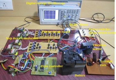
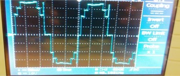
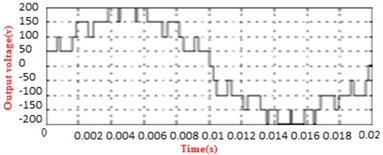
Fig. 33Nine level MLI: a) experimental output, b) simulation output, c) load current, d) THD analysis
a)
b)
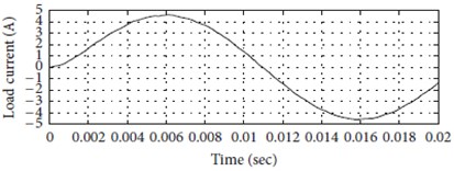
c)
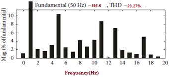
d)
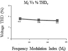
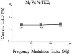
Fig. 33 shows the nine-level experimental output it have more harmonics compared with the 32 level based on the reduction of vibrations. Table 6 shows the Comparison of various parameters to measure vibration using THD analysis chart as shown in Fig. 34.
Table 6Comparison of various parameters to measure vibration
Parameter | Diode clamped | Developed H bridge | Torque ripple | Current ripple |
Proposed THD for level 31 (%) | 12.5 | 4.22 | 0.6 | 0.7 |
THD for level 17 (%) | 32.11 | 28.12 | 0.66 | 1.2 |
THD for level 27 (%) | 20.5 | 21.12 | 0.71 | 1 |
THD for level 9 (%) | 27 | 18 | 0.89 | 1.6 |
Table 7Comparison of converter for MLI
Particulars | Converter presented by Zhu et al. (2015) | Proposed converter for MLI |
Losses when converter operates in SD | 4.21 W | 6.42 W |
Losses when converter operates in MBCD | 1.69 W | 2.86 W |
Losses when converter operates in MBDD | 2.1 W | 3.52 W |
Total losses when converter operates in all distribution domains | 8 W | 12.8 W |
Average efficiency when converter operates in all distribution domains | 93.81 % | 90.47 % |
Total number of components | 11 | 12 |
Type of conversion | (Buck) | (Buck-Boost) |
Possibility of output voltage control | or | |
Driver circuit complexity | Complex | Simple |
Fig. 34THD analysis chart
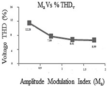
a)
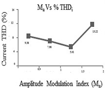
b)
c)
d)
4. Conclusions
The proposed Subsystem contains the hybrid quasi converters with two sources, namely wind and solar ones. Its source networks having boost abilities are used to step up the voltages from photovoltaic systems and from wind energy. In any case, the customary DC-DC systems have a few confinements to help the voltages, and there is discontinuity of input current and voltage and current burdens. To solve the above issues, adjusted and combinational source systems are fabricated to be utilized for distinguishable applications from customary systems with expanded effectiveness and even cost effective. The level of the harmonics and its supply power were analyzed and reduced. It is designed with both 17-level and 31-level diodes clamped based on the converter unit. The H bridge topology was developed with MATLAB/Simulink. Finally, the operation of total subsystem is verified based on the harmonic reduction. From the experimental results, it is concluded that the proposed Subsystem with the developed H bridge converter has the least total harmonic distortion as 4.22 % and 28.12 % for 31-level and 17-level MLI topology respectively.
References
-
Nejabatkhah F., Danyali S., Hosseini S. H., Sabahi M., Niapour S. M. Modeling and Control of New Three-input DC–DC Boost Converter for Hybrid PV/FC/battery power system. IEEE Transactions on Power Electronics, Vol. 27, Issue 5, 2012, p. 2309-2324.
-
Tibola G., Duarte J. L. Isolated bidirectional DC-DC converter for interfacing local storage in two-phase DC grids. 8th International Symposium on Power Electronics for Distributed Generation Systems (PEDG), Florianopolis, 2017.
-
Rahmati S. H. A., Zandieh M. New biogeography-based optimization (BBO) algorithm for flexible job shop scheduling problem. The International Journal of Advanced Manufacturing Technology, Vol. 58, Issues 9-12, 2012, p. 1115-1129.
-
Brandimarte P. Routing and scheduling in flexible job shop by tabu search. Annals of Operations Research, Vol. 41, Issue 3, 1993, p. 157-183.
-
Abd-Elazim S. M., Ali E. S. Hybrid particle swarm optimization and bacterial foraging for power system stability enhancement. Complexity, Vol. 21, Issue 2, 2015, p. 245-255.
-
Zhijun E., Fang D. Z., Chan K. W., Yuan S. Q. Hybrid simulation of power systems with SVC dynamic phasor model. International Journal of Electrical Power and Energy System, Vol. 31, Issue 5, 2009, p. 175-180.
-
Nabae A., Takahashi I., Akagi H. New neutral-point-clamped PWM inverter. IEEE Transactions on Industry Applications, Vol. 5, 1981, p. 518-523.
-
Xu G., Sha D., Xu Y., Liao X. Dual-transformer-based DAB converter with wide ZVS range for wide voltage conversion gain application. IEEE Transactions on Industrial Electronics, Vol. 65, Issue 4, 2018, p. 3306-3316.
-
Hariri A., Faruque M. O. Hybrid simulation tool for the study of PV integration impacts on distribution networks. IEEE Transactions on Sustainable Energy, Vol. 8, Issue 2, 2017, p. 648-657.
-
Yilmaz M., Krein P. T. Review of battery charger topologies, charging power levels, and infrastructure for plug-in electric and hybrid vehicles. IEEE Transactions on Power Electronics, Vol. 28, Issue 5, 2013, p. 2151-2169.
-
Shuai Z., Liu D., Shen J., Tu C., Cheng Y., Luo A. Series and parallel resonance problem of wideband frequency harmonic and its elimination strategy. IEEE Transactions on Power Electronics, Vol. 29, Issue 4, 2014, p. 1941-1952.
-
Odeh C. I., Anih L. U., Ejiogu E. C. 17-Level switched voltage source multi-level inverter topology with low-switching frequency control. Electric Power Components and Systems, Vol. 44, Issue 19, 2016, p. 2185-2197.
-
Odeh C. I. Improved three-phase, five-level pulse-width modulation switched voltage source inverter. IET Power Electronics, Vol. 8, Issue 4, 2015, p. 524-535.
-
Cui D., Ge Q. Novel hybrid voltage balance method for five-level diode-clamped converters. IEEE Transactions on Industrial Electronics, Vol. 65, Issue 8, 2018, p. 6020-6031.
-
Ho A. V., Chun T. W. Single-phase modified quasi-Z-source cascaded hybrid five-level inverter. IEEE Transactions on Industrial Electronics, Vol. 65, Issue 6, 2018, p. 5125-5134.
-
Dao N. D., Lee D. C. Operation and control scheme of five-level hybrid inverter for medium voltage motor drives. IEEE Transactions on Power Electronics, Vol. 33, Issue 12, 2018, p. 10178-10187.
-
Bharatiraja C., Ravi A., Banerjee S., Chakraborty A., Anupam A., Menon A. Hybrid cascaded multilevel inverter with diode assisted boosting network. Energy Procedia, Vol. 117, 2017, p. 1024-1031.
-
Deng Wu, Yao Rui, Zhao Huimin, Yang Xinhua, Li Guangyu A novel intelligent diagnosis method using optimal LS-SVM with improved PSO algorithm. Soft Computing, 2017, https://doi.org/10.1007/s00500-017-2940-9.
-
Deng Wu, Zhao Huimin, Zou Li, Li Guangyu, Yang Xinhua, Wu Daqing A novel collaborative optimization algorithm in solving complex optimization problems. Soft Computing, Vol. 21, Issue 15, 2017, p. 4387-4398.
-
Deng Wu, Zhang Shengjie, Zhao Huimin, Yang Xinhua A novel fault diagnosis method based on integrating empirical wavelet transform and fuzzy for motor bearing. Entropy, Vol. 6, 2018, p. 35042-35056.
-
Zhao Huimin, Yao Rui, Xu Ling, Yuan Yu, Li Guangyu, Deng Wu Study on a novel fault damage degree identification method using high-order differential mathematical morphology gradient spectrum. Entropy, Vol. 20, Issue 682, 2018, p. 1-18.
-
Zhao Huimin, Sun Meng, Deng Wu, Yang Xinhua A new feature extraction method based on EEMD and multi-scale fuzzy entropy for motor bearing. Entropy, Vol. 19, Issue 1, 2016, p. 14.
-
Deng Wu, Zhao Huimin, Yang Xinhua, Xiong Juxia, Sun Meng, Li Bo Study on an improved adaptive PSO algorithm for solving multi-objective gate assignment. Applied Soft Computing, Vol. 59, 2017, p. 288-302.
-
Sathish Kumar Shanmugam, Arumugam Senthilkumar Design and implementation of DC source fed improved dual-output buck-boost converter for agricultural and industrial applications. Journal of Vibroengineering, Vol. 19, Issue 8, 2017, p. 6433-6454.
