Abstract
The Proposed research deals implementation of standalone dynamic solar array fed permanent magnet synchronous motor drive using zero voltage resonant switch converter for the reduction of switching losses and oscillations. The closed loop control voltage strategy has been proposed for power flow management between solar photovoltaic (PV), battery, motor load and to maintain constant load voltage to perform continuous MPPT operation of solar PV. For improving the efficiency and to reduce vibration across the load SPV array fed Zero Voltage Switching (DISOZVS) Resonant Converter with permanent magnet synchronous motor (PMSM) drive is proposed. The DISOZVS resonant converter with suitable switching operation accomplishes for the purpose of reducing the Switching losses. The ZVS converter is constructed by a buck-boost circuit, which is operated as a buck circuit when charging and a boost circuit when discharging. So, we can use many power related systems, which improves efficiency, lower losses and higher performance. The various dynamics and oscillations of standalone SPV array is analysed in the proposed research. The performance of the proposed system is simulated in MATLAB/Simulink atmosphere and various parameters outputs are carried. A hardware prototype of the proposed system has been fabricated for the proposed converter and various analysis were incorporated. The working of the proposed scheme for the different levels of input solar insolation and Load power demand has been satisfactorily demonstrated for both simulation and experimental compared to conventional it results more efficient with reduced losses and oscillations.
Highlights
- Dual-input-single-output ZVS converter which has high efficiency, voltage gain, less complexity and low cost.
- B4 inverter has been used for fault tolerant control. it reduces switching current, frequency, high output voltage.
- Reduce the heat loss, which can increase the switches life time and also improves efficiency.
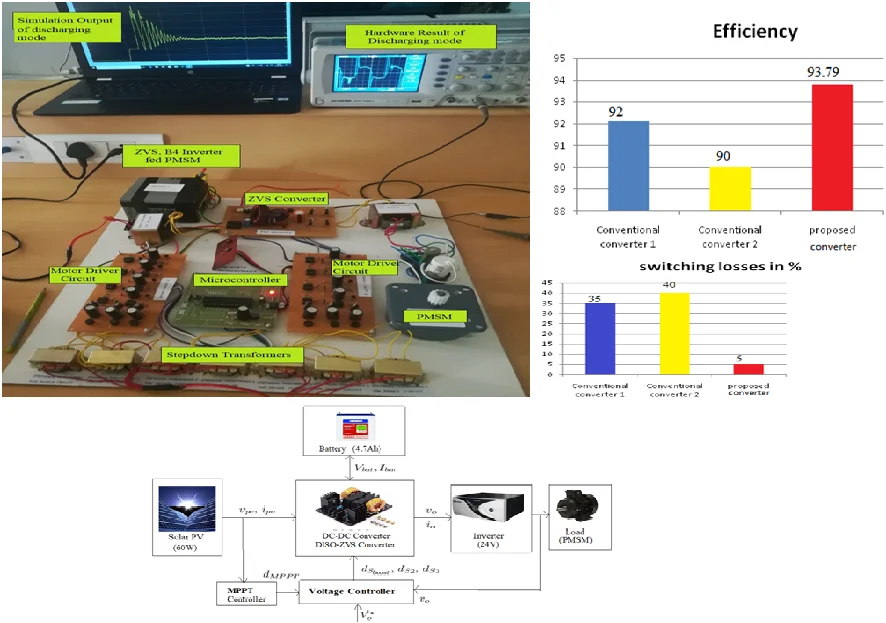
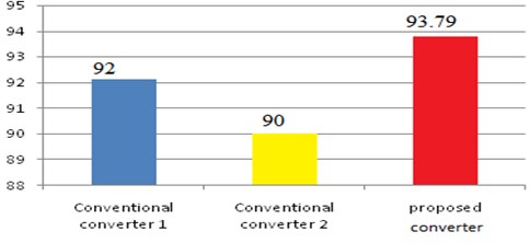
- The efficiency of the proposed DISOZVS converter is achieved about 93.79% by reducing the switching losses across the boost switch.
- The proposed research is used for One among the well-known applications of the PV power utilization is the water pumping applications powered by an electric motor.
1. Introduction
In recent days Bridling renewable electricity sources such as wind power, sun strength, tidal, and so forth. is essential for overcoming troubles because of international warming and environmental degradation resulting from using fossil fuels. Among all renewable strength assets, sun PV is abundant, has high strength density and is modular and scalable. Solar PV is used both in grid linked packages and standalone packages, it may be used in a huge variety of applications from a microwatt Internet of Thinks (IoT) implement to a megawatt scale solar PV plant [1, 2]. solar PV operates in an extensive range of DC voltages, at the same time as electrical and digital structures additionally have different tiers of DC voltage necessities [3].Subsequently, it’s far important to use power electronic interfaces for solar PV packages, for the reason that electricity from solar PV is intermittent in nature, it is necessary to mix electricity storage systems and different renewable electricity assets to maintain reliable operation for standalone PV structures. This may be executed through many single input two port DC-DC converters in parallel or multiport DC-DC converters. The centralized structure of multiport converters makes use of fewer switches, has compact shape, decrease cost, higher performance and avoids the want to use common unique structures compared to multiple single input/output DC-DC converters [4, 5] and [6]. Shen et al. [4] have proposed a three port converter incorporating solar PV, battery as power assets feeding DC hundreds with galvanic isolation. The manage shape worried a complex hybrid modulation technique (PWM + PFM) with gentle switching. Ray et al. proposed an included dual output DC-DC converter which had each buck and boost outputs using PWM to modify output voltages [7]. Various feasible topologies for multiport converters were discussed in [8]. However, using more than one inductor results in reduced converter size and cost. So as to overcome those problems, single inductor more than one enter/output topologies have been proposed. Unregulated inductor and couple of output DC-DC converters primarily based on equipment size, buck-boost enhance topologies had been proposed in diverse literature [9-13], this reduces the price, circuit complexity and consequences in greater performance. Nami et al. [14] have added a novel DC-DC multi-output increase converter that could percentage its total output among the special series of output voltages used in low and excessive strength packages. Considerably, two switches for one output are used and DC-DC multi-output control mechanism becomes complex. Further, the related output energy cannot provide individual regulation in a balanced way.
Boora et al. [15] also have illustrated a unique multi-output DC-DC converter topology, which has the talents of step-up and step-down conversion. In this topology, a couple of output voltages may be produced and might be utilized in various programs like multilevel converters with diode-clamped topology or electricity resources with distinct voltage tiers, but a couple of number of switches inside the converter outcomes in electricity losses. Patra et al. [16] have introduced a SIMO DC-DC converter with the functionality of producing greenback, boost, and inverted outputs simultaneously. Though, three switches for one output are needed for SIMO. This mechanism is appropriate most effective for the low output voltage and strength applications, and its strength conversion receives degraded as a result of the hard switching operation. Chen proposed [17] additionally have examined a more than one-output DC-DC converter with shared zero-converter switching (ZCS) lagging leg. Despite the fact that this converter with the tender-switching assets can reduce the switching losses, this integration scheme with three complete-bridge converters is greater complicated such that the purpose of high-efficiency power conversion is tough to be achieved, and its fee has an inevitable rise. Attributable to the drastic growth in the intake of strength for the beyond few decades, sources and environmental demanding situations are growing as much as be established, and therefore the strength minimizing time is one among the largest troubles desiring respond. Renewable power assets and the electric machines, inside the form of pollution less and greatly innovative electricity conveying devices with low noise characteristic, own a massive role in solving the difficulty. Most of the renewable resources, PV generation is unexpectedly getting vast popularity, crediting to the intrinsic advantages along with no fuel rate, no noise and put on as a result of non-inclusion of mobile components, lesser renovation and shortage of any inexperienced-house gasses [18].
One among the well-known applications of the PV power utilization is the water pumping applications powered by an electric motor. In this utility, the expenses of PV device and water pumps are expected to reduce greater steeply over the approaching few years, it isn't a surprise that the need for the PV energy turns into broadly spread. Those factors can make the PV water pumping systems greater economic inside the near destiny. In remote areas that are faraway, PV water pumping gadget may be utilized in several applications like household expenditure, water for irrigation, agricultural purposes, and village water supplies. The blessings of employing water pumps pushed via PV device consist of lesser upkeep, easy set up and robustness[19].An induction motor is appreciably hired in PV array pushed water pumping for the functions of irrigation and home makes use of as it’s miles suitable for programs in polluted and lone regions, lesser fee, reliability and occasional maintenance needs are proposed [20]. A DC motor is also utilized by Bhim singh [21] however because of the need for high protection demand and to the presence of the brushes and commutator, it isn't always suitable for water pumping. Consequently, a significant efficiency of a permanent magnet synchronous motor has stimulated the research specialists to apply this motor in places where a high energy submersible water pumping gadget is deployed. A few researches in the region of PV array fed water pumping utilising a synchronous reluctance motor and switched reluctance motor were carried out by researchers (Nabil et al. 2013) [22],but those dc motors have no longer won plenty popularity for PV array fed water pumping until now, likely owing to a completely excessive torque ripple and acoustic noise trouble this is gift with this drive. In contrast the BLDC motor has several advantages over conventional motor.
Like higher speed and torque traits, good performance and reliability, longer operation life, noise-free performance and much less electromagnetic interference proposed [23, 24]. Several researchers Luque et al. (2011) [25] have centered on this drive for PV array primarily based water pumping. A Permanent magnet Synchronous motor (PMSM) is used for driving the water pump depending on PV array that depicts its suitability for water pumping. At present more wide variety of variable velocity PMSM drives are developed into pump merchandise for growing the product overall performance and device effectiveness. A DC-DC converter is typically placed between the PV array and B6-Inverter fed PMSM pump for tracking the top of the line working factor of the PV array exploiting a MPPT method [26].
2. Materials and methods
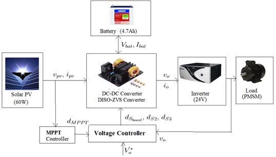
The proposed research indicates a new non-remoted Dual input Single Output Zero Voltage Switching Resonant Converter (DISOZVS) simply referred to as DISOZVS converter which has step-up and step-down conversion competencies. On this topology, special output voltages may be produced that is probably useful in several packages like diode-clamped multi-level inverters, multi-voltage DC-networks that deliver constant power with diverse demands and velocity control of PMSM. The sun PV module is the number one source of strength for the standalone PMSM load. The energy generated through the solar PV module for a given temperature and stage of irradiation relies upon on PV voltage and current drawn by the demand. Subsequently, a good way to do load matching, a Maximum Power Point Tracking (MPPT) manage is used to set the converter at Maximum Power Point (MPP) via various the obligation ratio of the proper transfer and for this reason the contemporary drawn by using the converter from the solar PV module. There are numerous algorithms used to tune the MPP like consistent voltage, perturb and observe, incremental conductance and beta method [25]. Among them, a simple perturb and observe (P&O) algorithm is chosen for the proposed device. The proposed block diagram using (DISOZVS) converter are shown in Fig. 1.
Fig. 1Proposed block diagram of DISOZVS converter
2.1. Conventional circuit diagram
The conventional circuit diagram is shown in Fig. 2. The researcher has proposed the parametric value of ( and ) of 24 V, 70 W solar PV module for the system and the same is modeled using the five parameter model [27]. The boost derived single inductor based dual input/output DC-DC converter (SI-DIO) used in the proposed power flow management system is shown in Fig. 2. It consists of diode Din which interfaces the solar PV module to the converter and also prevents reverse power flow to the solar PV module. The capacitor in is connected in parallel to the solar PV module to reduce the solar PV voltage ripples. The switches and diode is used to set the battery as an output to store excess solar PV power. The switch is used to set the battery as an input to supply power to the standalone DC load. The capacitor Co is connected across the output to reduce the output voltage ripples. The converter has two modes of operation namely dual output boost mode (DOBM) when the power from solar PV module exceeds DC load demand and dual input boost mode (DIBM) when there is a deficit. The circuit configuration for both the modes is shown in Fig. 2 [27].
Fig. 2Conventional schematic circuit diagram [27]
![Conventional schematic circuit diagram [27]](https://static-01.extrica.com/articles/20697/20697-img2.jpg)
During DOBM, the solar PV module acts as a power source feeding the battery through the switch and the DC load through the diode . The single inductor based dual IO removed (input/output) DC-DC converter has three states as shown in Fig. 2. In the first state, the inductor is charged by power from the solar PV module through switch . In the second state, switch is turned off and the inductor discharges to the DC load through the diode . In the third state, the surplus power is discharged to the battery by turning on the switch . Since, the required voltage of the standalone DC load is higher than that of the battery, the diode is reverse biased and the standalone DC load is cut off. Typical waveforms for the inductor current , the inductor voltage , the battery current and the output DC load voltage for this mode is shown in Fig. 2 [27].
Wu Deng proposed [28], an improved ant colony optimization (ICMPACO) algorithm based on the multi-population strategy, co-evolution mechanism, pheromone updating strategy, and pheromone diffusion mechanism is proposed to balance the convergence speed and solution diversity, and improve the optimization performance in solving the large-scale optimization problem. In the proposed ICMPACO algorithm, the optimization problem is divided into several sub-problems and the ants in the population are divided into elite ants and common ants in order to improve the convergence rate, and avoid to fall into the local optimum value. The pheromone updating strategy is used to improve optimization ability.
Wu Deng proposed [29] the improved PSO algorithm is used to optimize the parameters of least squares support vector machines (LS-SVM) in order to construct an optimal LS-SVM classifier, which is used to classify the fault. Finally, the proposed fault diagnosis method is fully evaluated by experiments and comparative studies for motor bearing for reduction of vibration.
Another algorithm MGACACO by Wu Deng [30] proposed makes use of the exploration capability of GA and stochastic capability of ACO algorithm. In the proposed MGACACO algorithm, the multi-population strategy is used to realize the information exchange and cooperation among the various populations. The chaotic optimization method is used to overcome long search time, avoid falling into the local extremum and improve the search accuracy.
Huimin Zhao, Wu Deng [31] proposed the EEMD method which is used to decompose the vibration signal into a series of intrinsic mode functions (IMFs) with a different physical significance. The correlation coefficient analysis method is used to calculate and determine three improved IMFs, which are close to the original signal. The multi-scale fuzzy entropy with the ability of effective distinguishing the complexity of different signals is used to calculate the entropy values of the selected three IMFs in order to form a feature vector with the complexity measure, which is regarded as the inputs of the support vector machine (SVM) model for training and constructing a SVM classifier (EOMSMFD based on EDOMFE and SVM) for fulfilling fault pattern recognition.
Wu Deng [32] proposed Another approach, the Alpha-stable distribution theory is used to replace the uniform distribution in order to escape from the local minima in a certain probability and improve the global search ability. Next, the DOADAPO algorithm is used to solve the constructed multi-objective optimization model of gate assignment in order to fast and effectively assign the gates to different flights in different time.
Huimin Zhao, Wu Deng [33] proposed damage degree identification method based on high-order difference mathematical morphology gradient spectrum entropy (HMGSEDI) is proposed in this paper to solve the problem that fault signal of rolling bearings are weak and difficult to be quantitatively measured. In the HMGSEDI method, on the basis of mathematical morphology gradient spectrum and spectrum entropy, the changing scale influence of structure elements to damage degree identification is thoroughly analyzed to determine its optimal scale range. The high-order difference mathematical morphology gradient spectrum entropy is then defined in order to quantitatively describe the fault damage degree of bearing. The discrimination concept of fault damage degree is defined to quantitatively describe the difference between the high-order differential mathematical entropy and the general mathematical morphology entropy in order to propose a fault damage degree identification method.
From various literature and analysis from the conventional system switching losses across the switch is high which makes the system with reduced efficiency and the dynamic solar array varies, to overcome this DISOZVS converter is proposed.
2.2. Battery management system for solar energy storage
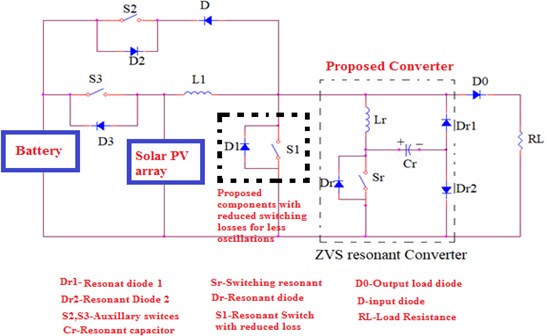
While partial shading occurs in the PV array, battery within the shape of strength storage device and a bidirectional DISOZVS converter are used to meet the call for strength. Among the various configurations of PV era, a stand-by myself PV-battery powered backup machine will be applied in diverse kinds of applications. A chargeable battery is generally exploited inside the device for electricity saving while the solar electricity generated exceeds the energy wished via the weight. On this the auxillary switch () is in an active part. The electricity stored can be useful in maintaining the gadget operation at the same time as the shading to the PV panel is executed. Hence the boost switch () is also in an energetic element. Two Power switches ( and ) used in the converter structure act as the leader controllable factors controlling the strength waft of the converter. The proposed schematic DISOZVS converter are shown in Fig. 3.
2.3. Proposed DISOZVS converter
Interval 1 (): at time , the lower switch is turned ON and the upper switch is turned OFF with diode , reverse biased as shown in Fig. 3. During this time interval the converter operates in boost mode and the inductor is charged and current through the inductor increases.[26]
Interval 2 (): during this interval both switches and is turned OFF. The body diode of upper switch starts conducting as shown in Fig. 3. The converter output voltage is applied across the motor. As this converter operates in boost mode is capable of increasing the battery voltage to run the motor in forward direction.
Interval 3 (): at time , the upper switch is turned ON and the lower switch is turned OFF with diode , reverse biased as shown in Fig. 3. During this time interval the converter operates in buck mode.
Interval 4 (): during this interval both switches and is turned OFF. The body diode of lower switch starts conducting as shown in Fig. 3.
Fig. 3Proposed circuit diagram of DISOZVS converter
2.3.1. Case 1: DISOZVS Converter modes of operation
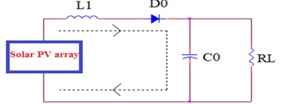
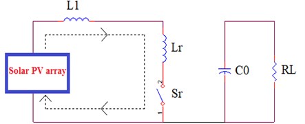
Mode A. In mode A, at the instant of time the solar PV source delivers the power to the inductor which is connected in series with the Solar PV source, so that the inductor gets charged and the energy is stored in the inductor at the dual output Boost Converter are shown in Fig. 4 and its dynamic equation are illustrated in Eqs. (1-2):
Fig. 4Mode A solar power charges inductor L1
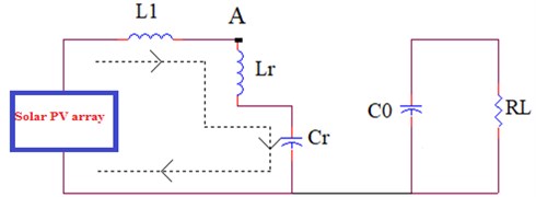
Mode B. In mode B, the resonant switch gets turned ON. At this instant of time the resonant inductor which is connected in series with the inductor and the Solar PV module, gets charged and stores energy when the inductor discharges. Meanwhile the inductors is again charged by the PV source and the energy is stored in the inductor . In this mode both the inductors and gets charged and stores energy as shown in Fig. 5 and its dynamic equation are illustrated in Eq. (3):
Fig. 5Mode B solar power charges inductor L1 and Lr
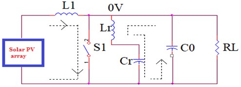
Mode C. In mode C, at the instant the potentials at inductor and resonant inductor is equal. Now the energy stored in both the inductor and the resonant inductor are discharged to charge the resonant capacitor which is connected in series with the resonant inductor and the energy gets stored in the capacitor as shown in Fig. 6 and its dynamic equation are illustrated in Eq. (4):
Fig. 6Mode C inductor L1 and Lr discharges to charge capacitor Cr
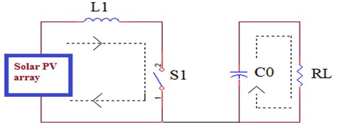
Mode D. In mode D, the auxiliary switch is turned on at the instant of time , the resonant capacitor gets discharged to attain zero potential at node A. The capacitor gets charged by the resonant capacitor . The capacitor is connected in parallel with the resonant inductor and resonant capacitor . The capacitor stores energy by the resonant capacitor . as shown in Fig. 7.
Fig. 7Mode D capacitor Cr discharges to charge capacitor Co
Mode E. In mode E, the auxiliary switch is turned ON, the capacitor which is connected in parallel with the resistive load RL. At the instant of time t₄, the energy stored in the capacitor is discharged to run the resistive load. In this mode, the power from the Solar PV module is sufficient to the resistive load RL as shown in Fig. 8 and its dynamic equation are illustrated in Eq. (5):
Fig. 8Mode E capacitor Co discharging mode
2.4. Control strategy of DISOZVS
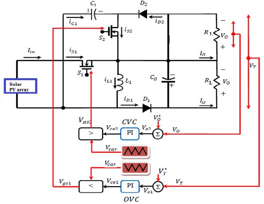
The voltage follower is required for controlling of DISOZVS converter operating at discontinuous conduction mode. For regulating the total output voltage of DISOZVS converter measurement sensors are required. Fig. 9 shows the closed loop control of DISOZVS converter. This control strategy comprises a voltage error generator, Output Voltage Controller (OVC), Capacitor Voltage Controller (CVC) and a PWM generator. The output voltage is generated by using the error generator comparison voltage are given in Eqs. (6-7):
where, – error control voltage, – error output voltage, – total output voltage, , – proportionality constant.
The 0.2, 0.1 are used for error control strategy which is given in Eq. (8):
Fig. 9Control strategy of DISOZVS
2.5. Analysis of power losses on DISOZVS
2.5.1. Resonant Switch conduction losses
During analysis of conduction, the is on at junction temperature and it is illustrated in the Eqs. (9-11). The delta value of inductor, capacitor are calculated and given in Eqs. (12-13):
The conduction of inductor, capacitor, switching currents of DISOZVS are shown in Fig. 10.
Fig. 10a) Conduction of inductor, capacitor, switching currents of DISOZVS, b) key waveforms of various parameters
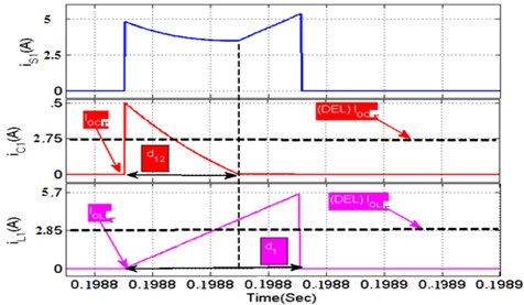
a)
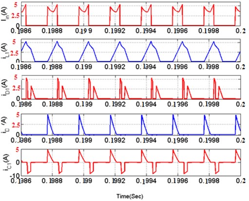
b)
The effectiveness of framework is indirect to the complete power. All output power, in the DISOZVS converter, such as conduction, exchanging, diode and inductor are indirect. Event of the conduction misfortunes is because of the declining voltage over the power semiconductor device just as the present move through the power semiconductor device striking in theme. Exchanging misfortunes are supported by the simultaneous event of voltage and current on the power semiconductor device while exchanging. The key waveforms of DISOZVS converter are appeared in Fig. 10(b). , , , , and are the current through the information supply, inductor , diodes and capacitor respectively. Evaluation of these misfortunes should be possible utilizing disentangled gadget models:
where is rise time, is fall time, refers tocurrent conduction of resonant switch () (refer Eq. (14)), stands for drain voltage of switch () and is operating switching frequency (5 kHz).
2.5.2. Gate loss on resonant switch
where, is output power of zero voltage resonant switch converter (30 W) and refers to total power losses.
2.6. Implementation of dynamic standalone solar array, battery power, four switch inverter fed PMSM drive
2.6.1. Case 2: battery charging mode
2.6.1.1. Mode F battery charging mode at
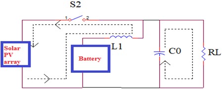
In mode F as shown in Fig. 11 the power generated at the solar PV module is excess for running the resistive load RL. Such that, the excess power from the PV source is used to charge the battery which is used as a backup source. At the instant the auxiliary switch is turned ON. The excess power from the solar PV source is used to charge the battery through the auxiliary switch .
Fig. 11Mode F solar power to RL load with charging battery
2.6.1.2. Mode () battery charging mode at PMSM
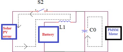
In mode as shown in Fig. 12 the power generated at the solar PV module is excess for running the PMSM motor with regulated voltage. Such that, the excess power from the PV source is used to charge the battery which is used as a backup source. At the instant the auxiliary switch is turned ON. The excess power from the solar PV source is used to charge the battery through the auxiliary switch .
Fig. 12Mode F1 solar power to motor load with charging battery
2.6.2. Case 3: mode G battery discharging mode at
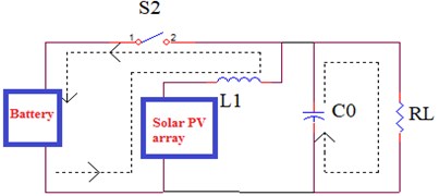
In mode G as shown in Fig. 13 the power from the solar PV source is insufficient to run the resistive load RL, such that the auxiliary switch is turned ON to draw power from the battery to run the resistive load RL and the auxiliary switch is also turned ON. At this instant, the power from the battery is used to charge the inductor and the inductor stores the energy from the battery.
Fig. 13Mode G solar power to RL with discharging battery
2.6.2.1. Mode battery discharging mode at PMSM
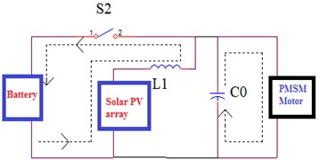
In mode as shown in Fig. 14 the power from the solar PV source is insufficient to run the motor, such that the auxiliary switch is turned ON to draw power from the battery to run the load and the auxiliary switch is also turned ON. At this instant, the power from the battery is used to charge the inductor and the inductor stores the energy from the battery.
Fig. 14Mode G1 solar power to motor load with discharging battery
2.6.3. Case 4: mode H battery in ideal condition at
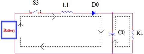
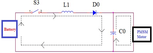
In mode H as shown in Fig. 15 the stored energy in the inductor is discharged through the diode which is forward biased and charges the capacitor . The capacitor is charged by both the solar PV source and the battery. The capacitor stores the energy and it discharges to run the resistive load RL. Thus, resistive load RL is run by the power from the solar PV source and the power drawn from the battery at the dual output boost mode.
Fig. 15Mode G Solar power to RL with ideal battery
2.6.3.1. Mode battery in ideal condition at PMSM
In mode as shown in Fig. 16 the stored energy in the inductor is discharged through the diode which is forward biased and charges the capacitor . The capacitor is charged by both the solar PV source and the battery. The capacitor stores the energy and it discharges to run the motor. Thus, load is run by the power from the solar PV source and the power drawn from the battery at the dual output boost mode.
Fig. 16Mode G1 solar power to RL with ideal battery
3. Results and discussions
3.1. Simulations results and discussions
To find out the performance of the proposed converter under the present control strategy, MATLAB simulations in different conditions have been performed. The simulation parameters such as input voltage (), input current (), input power (),output voltage, current and power of DC-DC converter (, and ) respectively, motor results such as speed, torque and stator current are used to evaluate the performance of the proposed system. The Simulation specifications of the proposed system are shown in Table 1.
Table 1Simulation specifications of the proposed system
Solar PV specifications | Motor specifications | ||
Open circuit voltage (VOC) | 32.8 V | Rated voltage | 24 V |
Short-circuit current (Isc) | 2.6 A | Rated current | 1.5 A |
Nominal voltage (Vmppt) | 24.65 V | Rated speed | 1200 RPM |
Nominal voltage (Imppt) | 2.44 A | Stator resistance | 1.4 ohms |
Maximum power (Pmppt) | 60.3 W | Number of poles | 6 |
Motor power | 36 W | ||
Battery parameters | Output parameters | ||
Nominal voltage | 24 V | Output PV voltage | 30 V |
Rated current | 4.7 AH | Output PV current | 0.5 A |
State of charge | 75 % | Output PV power | 15 W |
3.1.1. Solar PV input voltage ()
Fig. 17(a) determines the PV input voltage of the proposed system. From the input waveform of the DISOZVS it is referred that the voltage is about 18.3 V which changes according to the solar irradiation at 0.2 sec.
3.1.2. Solar PV input current ()
Fig. 17(b) determines the PV input current of the proposed system. From the input waveform of the DISOZVS it is referred that the current is about 1.6 A which changes according to the solar irradiation at 0.2 sec.
3.1.3. Solar PV input power ()
Fig. 17(c) determines the PV input power of the proposed system. From the input waveform of the DISOZVS it is referred that the power is about 29.25 W which changes according to the solar irradiation at 0.2 sec.
Fig. 17Solar PV DISOZVS input: a) voltage, b) current, c) power

a)

b)

c)
3.2. Proposed simulation output for battery
3.2.1. Battery voltage
Fig. 18 determines the Battery voltage of the proposed system. The waveform represents the output level of the battery voltage which is about 24 V.
3.2.2. Battery charging and disharging current
Fig. 19 determines the Battery current of the proposed system. The waveform describes the charging current is –0.4 A and discharging current is 0.6 A in the battery according to the load power requirements.
Fig. 18Solar PV battery output voltage

Fig. 19Solar PV power demand battery charging and discharging current

3.2.3. Battery charging and discharging power
Fig. 20 determines the battery power of the proposed system. The waveform describes the charging power is 17.5 W and discharging power is 14 W in the battery according to the load power requirements.
Fig. 20Solar PV power demand battery charging and discharging power

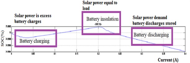
3.2.4. Battery state of charge
Fig. 21 determines the state of charging in Battery of the proposed system. The waveform describes the ideal, charging and discharging state in the battery.
Fig. 21Battery charging and discharging state of charge (SOC%)
3.3. Proposed simulation output for converter
3.3.1. Solar PV output voltage ()
Fig. 22(a) determines the DC voltage of the proposed system. The waveform represents the output DC voltage which is about 30 V in accordance with the PV source and the battery source.
3.3.2. Solar PV output current ()
Fig. 22(b) determines the DC current of the proposed system. The waveform represents the output DC current which is about 0.5 A in accordance with the PV source and the battery source.
3.3.3. Solar PV output power ()
Fig. 22(c) determines the DC power of the proposed system. The waveform represents the output DC power which is about 15 W in accordance with the PV source and the battery source which is used to run the load.
Fig. 22Solar PV DISOZVS output: a) voltage, b) current, c) power

a)

b)

c)
3.4. Proposed simulation output for motor parameters
3.4.1. Speed of a motor
Fig. 23(a) determines the motor speed of the proposed system. The waveform describing the speed of the PMSM drive is 1200 rpm which is operated by the converter output.
3.4.2. Torque (N-m)
Fig. 23(b) determines the motor torque of the proposed system. The waveform describes the torque obtained by the PMSM drive is 3.2 Nm which is operated by the converter output.
3.4.3. Direct current (), quadrature current ()
Fig. 23(c) determines the direct and quadrature current of the proposed system. The waveform describes the direct current (2.2 A) and quadrature current (–4 A) obtained in the PMSM drive which is operated by the converter output.
Fig. 23DISOZVS motor: a) speed, b) torque, c) Id, Iq

a)

b)

c)
3.4.4. Three phase motor current
Fig. 24 determines the motor three phase current of the proposed system. The waveform represents the Three phase current which is required to operate the PMSM drive.
Fig. 24DISOZVS motor stator three phase current

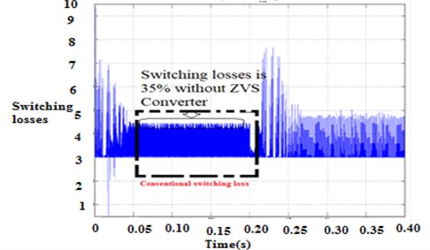
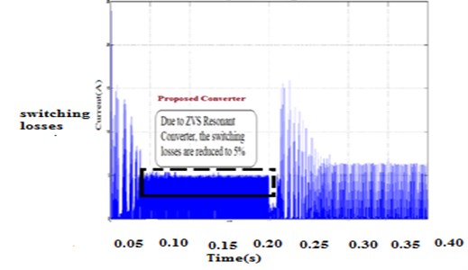
3.5. Comparison of simulation output of switching losses s1in percentage
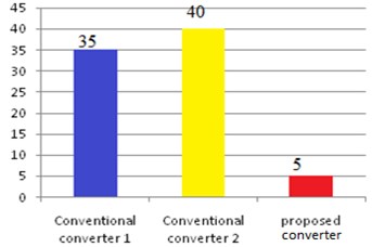
Fig. 25 determines the switching losses in proposed system. From the waveform it is referred that the switching losses is reduced to 5 % when compared with the conventional system.
3.6. Experimental analysis of DISOZVS and B4-inverter fed PMSM drive
The experimental verification is conducted for validating the proposed DISOZVS and B4-Inverter fed PMSM drive. The hardware of DISOZVS and B4-Inverter fed PMSM drive is presented in Fig. 26.
Fig. 25Comparison of conventional and proposed switching loss across S1
a)
b)
Fig. 26Experimental illustration for DISOZVS B4-inverter fed PMSM
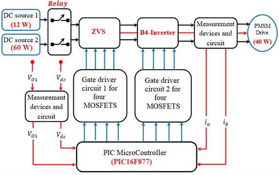
The hardware DISOZVS and B4-Inverter fed PMSM drive consists of 16-Bit digital signal Peripheral Interface Controller (PIC16F877) for DISOZVS control, B4-Inverter control, gate driver circuit for DISOZVS and B4-Inverter MOSFET’s. The feedback signals are processed with the help of measurement devices and circuit, and thereafter the control signals to the DISOZVS and B4-Inverter are transmitted by a PIC16F877 microcontroller. The DISOZVS converter is coupled among PV, Battery and load ports. A 36 W PMSM drive is powered by a B4-Inverter in the form of a load port of the new system. The DISOZVS converter input power is changed from 12 W to 60 W which in turn, is utilized for exemplifying the performance of the proposed system the experimental block diagram is shown in Fig. 26. Table 2 shows the experimental specifications.
Table 2Experimental specifications
Sl. no | Components | Range |
1. | Capacitor | 1000 µF, 63 V |
2. | PMSM | 220 V, 50 HZ, 60 RPM, 40 W |
3. | Inductor ( | 1.2 Mh |
4. | Diode (, ) | 5 A |
5. | Battery | 6V,4.7 Ah |
6. | Controller: PIC16F877 | 32-bit |
Fig. 27 determines the Switching pulses of Battery charging mode (, ). Here, the voltage level is equal to 15 V across the boost switch S1 and Battery charging switch .
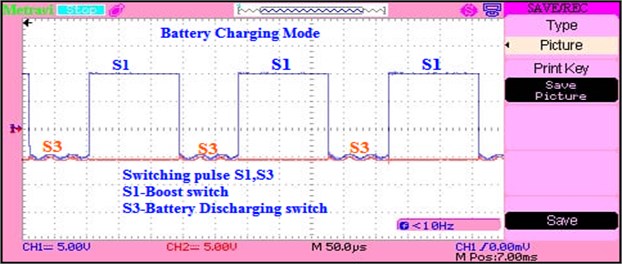
Fig. 28 determines the Switching pulses of Battery charging mode (, ). Here, the voltage level is equal to 15 V across the boost switch S1 and –5 V across the Battery discharging switch .
Fig. 27Switching pulses of battery charging mode (S1, S2)
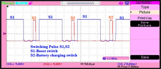
Fig. 28Switching pulses of battery charging mode (S1, S3)
3.6.1. Switching pulses of battery charging mode (, )
Fig. 29 determines the switching pulses of battery charging mode (, ). Here, the voltage level is equal to 15 V across the boost switch and auxiliary switch .
3.6.2. Switching pulses of inverter (, )
Fig. 30 determines the switching pulses of inverter (, ). Here, the voltage level is equal to 15 V across the inverter switch and switch .
3.6.3. Switching pulses of inverter (,)
Fig. 31 determines the Switching pulses of inverter (, ). Here, the voltage level is equal to 15 V across inverter switch and inverter switch .
Fig. 29Switching pulses of battery charging mode (S1, Sa)
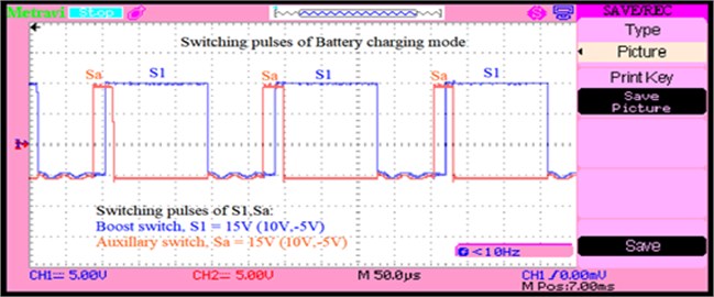
Fig. 30Switching pulses of inverter (S5, S6)
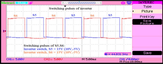
Fig. 31Switching pulses of inverter (S5, S7)

3.6.4. Switching pulses of inverter (, )
Fig. 32 determines the Switching pulses of inverter (, ). Here, the voltage level is equal to 15 V across inverter switch and inverter switch .
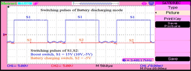
3.6.5. Switching pulses of battery discharging mode (, )
Fig. 33 determines the Switching pulses of battery discharging mode (, ). Here, the voltage level is equal to 15 V across boost switch and –5 V across the battery charging switch .
Fig. 32Switching pulses of inverter (S5, S8)

Fig. 33Switching pulses of battery charging mode (S1, S2)
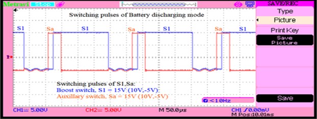
3.6.6. Switching pulses of battery discharging mode (,)
Fig. 34 determines the Switching pulses of battery discharging mode (, ). Here, the voltage level is equal to 15 V across boost switch and auxiliary switch .
Fig. 34Switching pulses of battery discharging mode (S1, Sa)
3.6.7. Switching pulses of battery discharging mode (, )
Fig. 35 determines the Switching pulses of battery discharging mode (, ). Here, the voltage level is equal to 15 V across boost switch and –5 V across the battery discharging switch .
3.6.8. Battery charging voltage
Fig. 36 determines the output waveform of battery charging voltage. Here, the voltage level in the battery is equal to 6 V at charging mode.
3.6.9. Battery discharging voltage
Fig. 37 determines the output waveform of battery discharging voltage. Here, the voltage level in the battery is equal to 12 V at discharging mode of operation.
3.6.10. Battery charging current
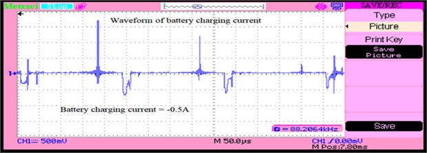
Fig. 38 determines the output waveform of battery charging current. Here, the current level in the battery is equal to –0.5 A at charging mode.
Fig. 35Switching pulses of battery discharging mode (S1, S3)
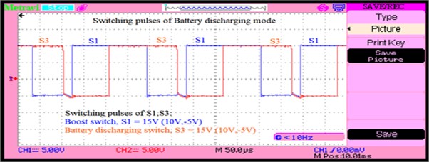
Fig. 36Battery charging voltage when excess power from source
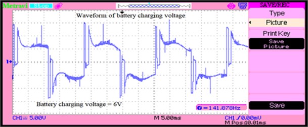
Fig. 37Battery discharging voltage when load power demands
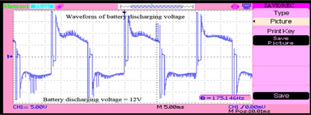
Fig. 38Battery charging current when excess power from source
3.6.11. Battery discharging current
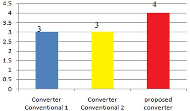
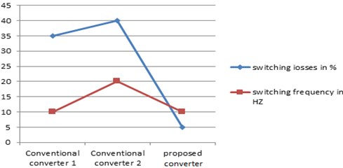
Fig. 39 determines the output waveform of battery discharging current. Here, the current level in the battery is equal to 6 A at discharging mode of operation. Fig. 40 shows the comparison of switches, switching losses of proposed DISOZVS with conventional converter. Fig. 41 curve represents the comparison of proposed DISOZVS with conventional converter switching Losses, switching frequency, efficiency. Comparison of conventional and proposed converter for various objects are shown in Table 3 which shows the proposed converter is more efficient. Table 4 shows the conduction of switches of proposed converter.
Fig. 39Battery discharging current when load power demands
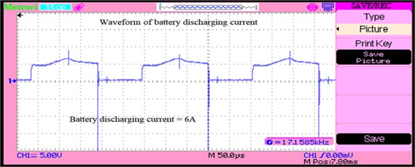
Table 3Comparison of conventional and proposed converter
S. No | Objects | Conventional converter 1 (Anand et al. 2018) [27] | Conventional converter 2 (Sathish Kumar et al. 2017, 2018) [18] | Proposed converter (DISO-DISOZVS) |
1 | No of switches | 3 | 3 | 4 |
2 | Efficiency | 92.1 | 91.4 | 93.79 |
3 | Switching losses in % | 35 % | 40 % | 5 % |
4 | Conversion topology | Boost | Buck-Boost | Buck-Boost |
5 | Switching frequency | 10 kHz | 20 kHz | 10 kHz |
Table 4Conduction of switches for proposed converter
Modes | Switch | Switch | Switch | Switch | Capacitor |
a | 0 | 0 | 0 | 0 | Off |
b | 0 | 0 | 0 | 1 | On |
c | 0 | 0 | 0 | 0 | ON |
d | 1 | 0 | 0 | 0 | ON |
e | 1 | 0 | 0 | 0 | Off |
f | 0 | 1 | 1 | 0 | off |
g | 1 | 0 | 0 | 0 | On |
h | 0 | 0 | 0 | 0 | On |
Fig. 40Comparison of: a) switches, b) switching losses proposed DISOZVS with conventional converter
a)
b)
Fig. 41Comparison of proposed DISOZVS with conventional converter: a) switching losses and switching frequency, b) efficiency
a)
b)
3.7. Prototype experimental test set up for proposed DISOZVS converter
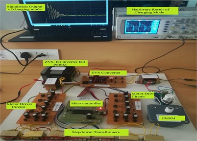
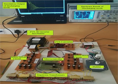
A 36 W PMSM drive is powered by a solar, battery fed B4-Inverter to the load port of the new system is proposed works efficiently. The DISOZVS converter input power is changed from 12 W to 60 W which in turn, is utilized for exemplifying the performance of the proposed system experimental solar and battery power with charging, discharging, ideal compared with simulation are shown in Figs. 42-44.
Fig. 42Prototype test set up for battery ideal mode of operation to PMSM drive
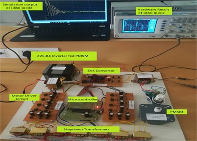
Fig. 43Prototype test set up for battery charging mode of operation to PMSM drive
3.8. Performance of DISOZVS converter under step change in load condition
Fig. 45 determines the performance of DISOZVS Converter under step change in input condition using PMSM drive. At the point when load protections 30 Ω (100 % load) is considered from 0 to 0.2 Sec. At a specific time, for example from 0.2 Sec to 0.4 Sec, load protections is all of a sudden diminished from 100 % to half (60 Ω) condition as appeared in Fig. 46(a). The yield voltage of the DISOZVS converter is wanted to be managed on (30 V). The yield voltage () is followed the reference esteem () with least relentless state blunder as appeared in Fig. 46(b).
Fig. 44Prototype type set up for battery discharging mode of operation to PMSM drive
Subsequently, the yield current () magnitude variation checks the proposed DISOZVS converter closed circle execution as appeared in Fig. 46(c). The time area investigation like over shoot, rise time, settling time, postponed time and steady state error, for yield voltage (), under advance change in input/load conditions at comparison with switching frequency toe reduce noise and oscillations in pmsm is appeared on Table 5.
Fig. 45Performance of DISOZVS converter under step change in input condition using PMSM drive


Table 5Change in input/load conditions for reduction of oscillations and noise in PMSM drive
At initial step input | Input voltage (V) | Load (%) | Output voltage (V) | Peak overshoot | Peak rise (ms) | Peak fall (ms) | Delay Time (ms) | PMSM drive | Frequency |
Input | 17 | 100 | 0-30 | 15 | 2.44 | 124 | 2.5 | Half value 20 W | 10 kHz |
24 | 100 | 30 | 7 | – | 93 | – | Full value 40 W | 10 kHz | |
Load | 17 | 100 | 0-30 | 14 | 2.4 | 124 | 2.5 | Half value 20 W | 10 kHz |
12 | 50 | 30 | 1.1 | 1.7 | 48 | – | Full value 40 W | 10 kHz |
Fig. 46Performance of DISOZVS converter under step change in load condition using PMSM drive

a)

b)

c)
4. Conclusions
The DC to DC converter is advantageous in renewable energy system at different input condition along with low cost conversion circuit. Since single input single output DC-DC converter are more complicated and expensive. The proposed research utilizes Dual-input-single-output ZVS converter which has high efficiency, voltage gain, less complexity and low cost. In addition to that B4 inverter has been used for fault tolerant control. it reduces switching current, frequency, high output voltage. We can reduce the heat loss, which can increase the switches life span. It also reduces the cost and improves efficiency, but also improves the performance of the system. Permanent magnet synchronous motor are compact, needs low maintenance and highly reliable, so it is proposed and convenient result were carried out. Thus, hardware implementation and MATLAB simulation verifying the feasibility of the system has carried out. The efficiency of the proposed DISOZVS converter is achieved about 93.79 % by reducing the switching losses across the boost switch. The implementation of the proposed work is practically used for industrial and agricultural application.
References
-
Liu X., Sinencio S’anchez E. A highly efficient ultralow photovoltaic power harvesting system with MPPT for internet of things smart nodes. IEEE Transactions on Very Large-Scale Integration (VLSI) Systems, Vol. 23, Issue 12, 2015, p. 3065-3075.
-
Ito M., Kato K., Sugihara H., Kichimi T., Song J., Kurokawa K. A preliminary study on potential for very large-scale photovoltaic power generation (VLS-PV) system in the Gobi Desert from economic and environmental viewpoints. Solar Energy Materials and Solar Cells, Vol. 75, Issues 3-4, 2003, p. 507-517.
-
Xu C. D., Cheng K. W. E. A survey of distributed power system – AC versus DC distributed power system. 4th International Conference on Power Electronics Systems and Applications, 2011.
-
Sun X., Shen Y., Li W., Wu H. A PWM and PFM hybrid modulated three-port converter for a standalone PV/battery power system. IEEE Journal of Emerging and Selected Topics in Power Electronics, Vol. 3, Issue 4, 2015, p. 984-1000.
-
Liu Y. C., Chen Y. M. A systematic approach to synthesizing multi input dc-dc converters. IEEE Transactions on Power Electronics, Vol. 24, Issue 1, 2009, p. 116-127.
-
Chen Y. M., Huang A. Q., Yu X., A. high step-up three-port DC-DC converter for stand-alone PV/battery power systems. IEEE Transactions on Power Electronics, Vol. 28, Issue 11, 2013, p. 5049-5062.
-
Ray O., Josyula A. P., Mishra S., Joshi A. Integrated dual-output converter. IEEE Transactions on Industrial Electronics, Vol. 62, Issue 1, 2015, p. 371-382.
-
Wu H., Zhang J., Xing Y. A family of multiport buck-boost converters based on DC-link-inductors (dlis). IEEE Transactions on Power Electronics, Vol. 30, Issue 2, 2015, p. 735-746.
-
Ki W.-H., Ma D. Single-inductor multiple-output switching converters. 32nd Annual Conference on Power Electronics Specialists, 2001, p. 226-231.
-
Bandyopadhyay S., Chandrakasan A. P. Platform architecture for solar, thermal, and vibration energy combining with MPPT and single inductor. IEEE Journal of Solid-State Circuits, Vol. 47, Issue 9, 2012, p. 2199-2215.
-
Benadero L., Moreno Font V., Giral R., Aroudi A. E. Topologies and control of a class of single inductor multiple-output converters operating in continuous conduction mode. IET Power Electronics, Vol. 4, Issue 8, 2011, p. 927-935.
-
Jiang W., Fahimi B. Multiport power electronic interface – concept, modelling, and design. IEEE Transactions on Power Electronics, Vol. 26, Issue 7, 2011, p. 1890-1900.
-
Moon Y. J., Roh Y. S., Gong J. C., Yoo C. Load-independent current control technique of a single-inductor multiple-output switching DC-DC converter. IEEE Transactions on Circuits and Systems II: Express Briefs, Vol. 59, Issue 1, 2012, p. 50-54.
-
Nami A., Zare F., Ghosh A., Blaabjerg F. Multi-output dc-dc converters based on diode-clamped converters configuration: topology and control strategy. IET Power Electronics, Vol. 3, Issues 2, 2010, p. 197-208.
-
Boora A., Zare F., Ghosh A. Multi-output buck-boost converter with enhanced dynamic response to load and input voltage changes. IET Power Electronics, Vol. 4, Issue 2, 2011, p. 194-208.
-
Patra P., Patra A., Misra N. A single-inductor multiple-output switcher with simultaneous buck, boost and inverted outputs. IEEE Transactions on Power Electronics, Vol. 27, Issue 4, 2012, p. 1936-1951.
-
Chen Y., Kang Y., Nie S., Pei X. The multiple-output DC-DC converter with shared ZCS lagging leg. IEEE Transactions on Power Electronics, Vol. 26, Issue 8, 2011, p. 2278-2294.
-
Sathish Kumar Shanmugam, Meenakumari Ramachandran Design and implementation of embedded processor based brushless motor drive using lead acid battery as source with lithium ion capacitor. Indonesian Journal of Electrical and Computer Science, Vol. 14, Issue 3, 2015, p. 455-469.
-
Sathish Kumar Shanmugam, Meenakumari Ramachandran Design and implementation of six switch three phase inverter BLDC motor drive for commercial applications. Asian Journal of Research in Social Sciences and Humanities, Vol. 6, Issue 7, 2016, p. 1301-1310.
-
Shanmugam S., Ramachandran M., Kanagaraj K., Loganathan A. Sensorless control of four-switch inverter for brushless DC motor drive and its simulation. Circuits and Systems, Vol. 7, Issue 6, 2016, p. 726-734.
-
Kumar R., Singh B. BLDC motor-driven solar PV array-fed water pumping system employing zeta converter. IEEE Transactions on Industry Applications, Vol. 52, Issue 3, 2016, p. 2315-2322.
-
Mazliza Abdul Halim, Muhamad Nabil Hidayat, Mohammad Nawawi Seroj implementation and analysis of a half-bridge series-parallel LLC loaded resonant DC-DC converter for low power applications. IEEE International Conference on Power Electronics and Drive Systems, 2013, p. 634-638.
-
Sathishkumar S., Meenakumari R., Jobanarubi E., Anitta P. J. S., Ravikumar P. Microcontroller based BLDC motor drive for commercial applications. power electronics and renewable energy systems. Lecture Notes in Electrical Engineering, Springer, New Delhi, Vol. 326, 2015, p. 829-841.
-
Shao H., Li X., Tsui C. Y., Ki W. H. A novel single-inductor dual-input dual-output DC-DC converter with PWM control for solar energy harvesting system. IEEE Transactions on Very Large-Scale Integration (VLSI) Systems, Vol. 22, Issue 8, 2014, p. 1693-1704.
-
Luque A., Hegedus S. Handbook of Photovoltaic Science and Engineering. John Wiley and Sons, 2011.
-
Shanmugam S., Meena Kumari R. Design and Implementation of modified buck boost converter fed B4 inverter for brushless dc motor drive using low cost DSPIC controller. Asian Journal of Research in Social Sciences and Humanities, Vol. 6, Issue 10, 2016, p. 1079-1101.
-
Anand I., Subramaniam Senthilkumar, Dipankar Biswas, Kaliamoorthy M. Dynamic power management system employing single stage power converter for standalone solar PV applications. IEEE Transactions of Power Electronics, Vol. 33, Issue 12, 2018, p. 10352-10362.
-
Deng Wu, Xu Junjie, Zhao Huimin An improved ant colony optimization algorithm based on hybrid strategies for scheduling problem. IEEE Access, Vol. 7, 2019, p. 20281-20292.
-
Deng Wu, Yao Rui, Zhao Huimin, Yang Xinhua, Li Guangyu A novel intelligent diagnosis method using optimal LS-SVM with improved PSO algorithm. Soft Computing, Vol. 23, Issue 7, 2019, p. 2445-2462.
-
Deng Wu, Zhao Huimin, Zou Li, Li Guangyu, Yang Xinhua, Wu Daqing A novel collaborative optimization algorithm in solving complex optimization problems. Soft Computing, Vol. 21, Issue 15, 2017, p. 4387-4398.
-
Deng Wu, Zhang Shengjie, Zhao Huimin, Yang Xinhua A novel fault diagnosis method based on integrating empirical wavelet transform and fuzzy for motor bearing. Entrophy, Vol. 6, 2018, p. 35042-35056.
-
Deng Wu, Zhao Huimin, Yang Xinhua, Xiong Juxia, Sun Meng, Li Bo Study on an improved adaptive PSO algorithm for solving multi-objective gate assignment. Applied Soft Computing, Vol. 59, 2017, p. 288-302.
-
Zhao Huimin, Sun Meng, Deng Wu, Yang Xinhua A new feature extraction method based on EEMD and multi-scale fuzzy entropy for motor bearing. Entropy, Vol. 19, Issue 1, 2016, p. 14.
