Abstract
The paper represents mathematical model and formulas developed for project calculations which are applied to sealed electronic units and provide assessing strength of passive electronic components having revolution shape (capacitors, resistors, diodes, pins, etc.). The stress calculation has been produced for materials of resistor and compound in the temperature interval (from –60 to +70°C) along the radius of resistor and compound.
1. Introduction
Modern development of electronics, that applies cutting-edge integrated and module assemblies, and tendency to micro-levels for reaching small and light high-density assemblies have posed new problems for developers to solve, one of which is to provide mechanical strength and reliability [1].
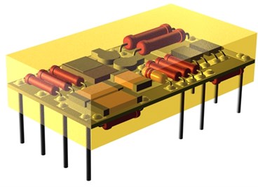
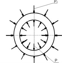
A lot of modern electronic units are performed as a sealed polymer bar with numerous inclusions as components and printed circuit boards with connecting pins and contact pads, which can be considered as a whole body – a composition consisting of many materials united in one (Fig. 1).
Fig. 1Sealed unit
Using such units made from new non-metallic materials with insufficiently studied physical and mechanical properties and applied in engineering of rockets, airplanes, machines, ships, radar-tracking stations and others, which work in conditions of temperature drops (thermal impacts from -60 to +70°C), causes strain which frequently breaks electronic components or their sealing [2].
This causes the necessity to develop mathematical models for estimating strength of passive electronic components sealed with compound what allows reasonable selecting contacting materials, specifying structural dimensions and spacing components inside the volume of compound on one hand and on the other hand to develop experimental methods, which allow assessing stress condition of passive components.
2. Developing calculative scheme
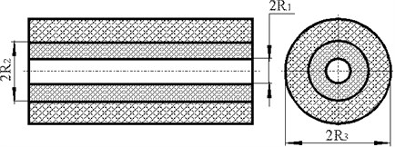
In the most general case cylindrical component (capacitor, resistor, pin) is coated by irregular compound layer. Imaginary circle of radius equal to minimal distance from component axis to the outer wall of the unit (Fig. 2) will select compound cylinder around electronic component in order to focus study on interaction between only selected layer of compound and the electronic component. Then calculative scheme can obviously be considered an axially symmetric problem of two cylindrical bodies to have contact interaction (Fig. 3) [3].
Fig. 2Creating calculative scheme: 1 – compound, 2 – selected compound cylinder, 3 – passive electronic component
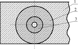
Fig. 3Electronic component coated by layer of compound
Solving this problem may be expected to have contracting and tension loads appeared in the bound between component and compound both in the passive electronic component and the compound under contact pressure caused by difference of coefficients of linear thermal expansion and other physical and mechanical characteristics of materials of component and compound at the temperature changes. Thus, in general, solving this problem is possible by using Lyame-Gadolin theory for strength calculation (theory of built-up barrels of artillery cannons) [4]. Although the nature of acting forces at this instance is different: for a cannon – it’s a pressure of powder gases inside the barrel, and for passive electronic component sealed by compound – it’s pressure in the bound of passive electronic component and compound; the basic part of solution is generalized to calculative scheme as axisymmetric problem.
3. Assessment of stress in electronic component and compound
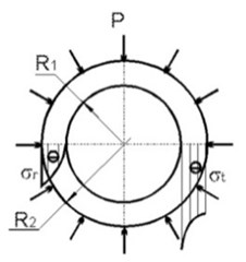
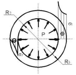
In the common case the interaction between electronic component and coating compound considers electronic component to be loaded over external surface by contact pressure , and over internal one by atmospheric pressure , and compound cylinder to be loaded over internal surface by contact pressure and over external surface by pressure equal the pressure outside (Fig. 4).
Fig. 4Load scheme of internal: a) and external, b) cylinders
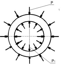
a)
b)
Assuming deducing cumbersome formulas the only final solution of the problem by using theory for thick-wall cylinders is represented. The formulas for radial stress , tangential stress and radial strain in material of electronic component (1-3) and compound (4-6) are represented in accordance to [4] as:
where , – Poisson's ratios of component and compound materials correspondingly; , – elasticity modulus of component and compound materials; , – coefficient of linear expansion of component and compound materials; , – internal and external radius of electronic component; , – internal and external radius of compound; – variable radiuses: , ; (Fig. 3), , , , – temperature integrals.
Temperature drops , present in formulas of thermal integrals (and stresses , ) are defined as: , , where – temperature of cylindrical surface of radius in the moment of time , which is counted from the moment to bring the item from the constant temperature into the temperature . is assumed to be the initial temperature of the body in calculations [5].
The formulas given above get significantly simplified if to neglect low environmental pressures and in comparison with much higher contact pressure .
For the stabilized temperature drop when temperature of the whole item reaches temperature, Eqs. (1)-(6) for calculating stress and strain become stresses and strains in the material of electronic component:
stresses and strains in the material of compound:
Stress diagrams in electronic component and compound are shown in Fig. 5.
Fig. 5Diagrams of tangential and radial stresses in materials of: a) internal, b) external cylinders
a)
b)
Analyzing formulas (7, 8, 10, 11) testified that if external radius of compound cylinder were 4 times greater than one of the component its further increasing would result in only 1/16 strain increment of the maximal. That's why compound cylinder can be considered as that with endless large wall at 5-6 % error tolerance. That provides strength calculation of sealed component irrespective to sealing compound profile by formulas (7, 8, 10, 11) in only condition that compound thickness is 4 times greater that component's external radius. It’s also clear that at the specified relation between thickness of compound and external radius of electronic component solution can be limited to axisymmetric problem since increasing pressure from compound out of the zone of selected cylinder will be insignificant in comparison with maximal one found by solving symmetric problem and may be neglected in engineering calculations [6].
4. Determining contact pressure
All previously represented formulas aimed at finding stress and strain of electronic component and compound are function of contact pressure . It should be found by considering condition of joint strain of electronic component and compound. Within the electronic component and compound structure at their sufficient adhesion they are joined and can strain only together. The condition of joint strain is:
Substituting into this formula strains of electronic component and compound in their bound from formulas (9) and (12) and solving equation relative to contact pressure (pressures and are neglected) results in equation (14):
5. Example of stress calculation in resistor OMLT-0.125 sealed with compound EZK-25 in sealed unit ZU5.760.001 at the stabilized temperature drop
The strength of resistor OMLT-0.125 sealed with compound EZK-25 will be calculated using given formulas in the temperature diapason 130°С (from +70°С to –60°С) along the radius of resistor and compound. The calculation is produced at regular thickness of compound layer and the range of fixed values of compound thickness taken from practice. Those are most unfavorable (from the point of view of strength) conditions when structure is taken from one temperature into the another. That’s why the structure which appeared to have sufficient strength in extreme conditions can be assumed to guarantee its reliability in normal conditions. Calculation is produced using the following data gathered on laboratory tests:
resistor – 0.292; 13.1·1010·N/m2; 6 10-6 deg-1; 0.2 mm; 0.75 mm;
compound – 0.3; 1.21·1010·N/m2; 45 10-6 deg-1; 0,75 mm; 1-10 mm.
Results of calculations are shown in graphs (Fig. 6, 7) where radiuses are traced on abscissa axis, and values of tangential and radial stresses in material of resistor or compound – on ordinate axis.
As materials of resistor and compound are in complicated stressed condition so their strength assessment should be performed by using strength theory [4]. Using third strength theory or theory of greatest tangential stresses for assessing strength of compound and ceramics of resistor represents the most interest.
Speaking specifically both materials the resistor and the compound are in three-dimensional stress but as the absolute value of longitudinal stress is significantly less than radial and tangential stresses so it can be neglected and the stress condition can be assumed as two-dimensional. Then, as by the absolute value so for compound cylinder and the strength condition is:
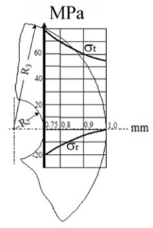
Fig. 6Stress diagram along the radius of resistor at various thickness of compound cylinder R3:––– R3= 1 mm, - - - - R3= 2 mm, - - · - - R3= 3 mm, - · · - · R3= 10 mm
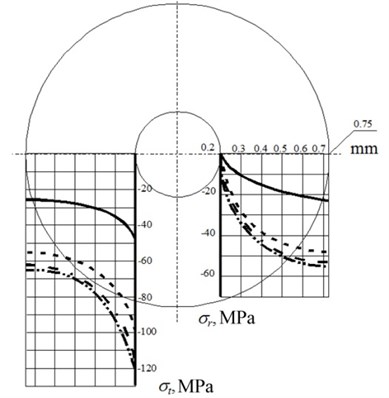
Fig. 7Stress diagram along the radius of compound at various thickness of compound cylinder: a) R3= 1.0 mm, b) R3= 2.0 mm, c) R3= 10.0 mm
a)
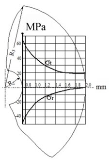
b)
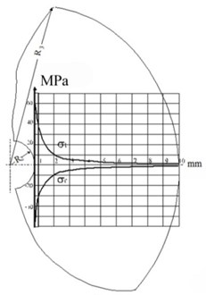
c)
Thus, the greatest equivalent stresses in compound will appear on the internal surface of compound cylinder and will always be greater, by the absolute value, than contact pressure. The residual strain in compound will appear when reaches the yield limit and increasing compound thickness will have no effect.
Indeed, let , meaning that compound thickness grows infinitely, then strength condition by the 3rd strength theory will appear to be:
When , we get , meaning that although infinitely thick layer of compound it won’t sustain the contact pressure producing stress exceeding the half of tension ultimate strength of compound.
Analogous results can be obtained for ceramic cylinder also.
6. Conclusion
On the basis of third strength theory improving strength of electronic component – compound system requires designing and using ceramics and compound to have yield limit and ultimate strength as high and stable as possible.
However, using strength theory in considered case won’t guaranty the accurate strength assessment.
If this is added by the fact that used ceramics, fragile initially, at -60 deg C and three-dimensional stress condition, what is round compression, can act as a plastic material, and compound conversely may become fragile, so it would be more reliable to assess experimentally measured stresses in compound and resistor against ultimate stresses, those which are destructive, measured in stress conditions close to operational. However this comment goes beyond this paper and will be discovered in the further publications.
References
-
Royzman V. P. Problem of strength reliability in radioelectronics. Technology and Construction in Electronic Devices, Odessa, “Polytechperiodica” Publishing House, 2005, Number 6, p. 6-12, (in Russian).
-
Kamburg V. G., Kovtun I. I., Grigorenko S. A. Influence of temperature to mechanical strength of passive electronic components, which are hermetized by compound. Reliability and Quality, Penza, Publishing House of Penza State University, 2000, p. 348-351, (in Russian).
-
Royzman V., Grigorenko S. Strength of passive electronic components hermetized by compound at thermal impacts. Herald of the Lvov Polytechnical State University “Radioelectronics and Telecommunications”, 2000, Number 387, p. 265-270, (in Ukrainian).
-
Pisarenko G. S., Kvitka O. L., Umanskiy E. S. Support of Materials. Handbook for students of mechanical departments of higher educational institutions, Kiev, Higher School Publishing House, 2004, 655 p., ISBN 966-642-056-2, (in Ukrainian).
-
Petraschuk S. A., Kofanov Yu. N., Royzman V. P. Solution of the problem of heat conduction in hermetized module at non stationary temperatures. Herald of Khmelnitskiy National University, Section of Technical Sciences, Vol. 6, 2011, p. 147-151, (in Russian).
-
Petrashchuk S. A., Kovtun I. I. Theoretical and experimental evaluation of strain in components under thermal impact. Proceedings of the International Conference “Science and Education”, Colombo, Sri Lanka, February 12 – 22, 2010, p. 79-84.
About this article

