Abstract
Energy harvesting properties of PVDF layers partially covered on double-curved shallow shells are studied. Firstly, the analytical expressions of voltage on the PVDF layers induced by shell vibration are derived; then the contribution to the voltage from vibrations in different directions is explored and also the effect of geometric parameters is analyzed. The results obtained theoretically indicate that: (1) The PVDF layers used on curved surface possess higher energy harvesting capabilities than those used on planar surface. (2) With the decreasing of radius of the shell, the energy harvesting capability of the PVDF layers is improved. (3) The energy harvesting ability of the laminated PVDF layers is better than that of single layer when laminated layers are connected in series mode. To validate the analytical results, energy harvesting experiments of PVDF layers on a straight beam and a curved beam are carried out comparatively. The voltage induced by vibration of the curved beam is much higher than that produced by the straight beam and the energy harvesting rate of PVDF layers on the curved beam is more rapidly than that on the straight beam. Furthermore, the voltage on the laminated PVDF layers in series connection is almost the summation of the voltages of PVDF layers which work separately. The results obtained experimentally are in agreement with those obtained analytically.
1. Introduction
With the development of low-power consumption technique used in microelectronic, wireless-transmission and microelectromechanical systems, the technique of capturing energy from the environment is becoming a research hot spot. Piezoelectric materials, such as PZT and PVDF layers, are good materials in energy harvesting due to their high efficiency in electromechanical conversion, strong anti-interference ability and ease to realize miniaturization. One easy mode to convert mechanical energy into electric energy by PZT or PVDF layers is to install them on the surface of the structures directly, which has little influence on the shape and properties of base structures.
In the past decade, the energy harvesting techniques using PZT or PVDF layers have been investigated extensively [1-3], and the research work can be divided into three aspects as following: (1) Modeling for the energy harvesting structures. (2) Design of the energy harvesting circuits. (3) Design and application of all kind of harvesters. In the modeling of the energy harvesting structures, beam [4-9] or plate [10-12] structures are chosen as the base structures in most research and the characteristics of PZT or PVDF layers on planar beams or plates have been explored comprehensively.
The applications of piezoelectric materials on structures with curved surfaces mostly focused on the actuators and vibration control. In our previous work, the characteristics of laminated PVDF layers and vibration control of cylindrical shells [13, 14], paraboloidal shells [15] and double curved shallow shells [16] have been studied, the theoretical and experimental results indicate that the electromechanical coupling characteristics of PVDF layers employed on curved surfaces are significantly different from that employed on plane surfaces; also the actuation ability of PVDF layers on curved surface is much higher than that on plane surface and the curvature of base structure has significant influence on the actuation property. Moreover, we realized that the characteristics of piezoelectric layers used on plane surfaces structures cannot be applied directly to that used on the curved surface structures. In energy harvesting, the piezoelectric effect is used, although it is not the same as the inverse piezoelectric effect used in actuators, the deformation of the curved structure is coupled inevitably with piezoelectric layers. Whether the PVDF layers used on curved surface possess outstanding ability in energy harvesting as they are used as actuators on curved structures? How do the parameters of curved structures influence the energy harvesting capability of PVDF layers? These are tempting problems to be explored.
To the best knowledge of the author, research work about energy harvesting employing structures with curved surface is still very scarce till now. Yoon [17] et al studied the charge generation and harvesting characteristics of an initially curved PZT unimorph structure. Mossi [18] et al used a thin unimorph prestressed bender to harvest energy and the effect of different parameters on energy harvesting is discussed. Huang [19] et al laminated piezoelectric sensor segments on a circular cylindrical shell and studied the electromechanical coupling effect of the system. In [17-19], all the base structures are curved only in one direction.
In this study, laminated PVDF layers are partially covered on the surface of a double-curved shallow shell to harvest the vibration energy. Analytic expressions of the voltage produced on the PVDF layers are derived. The influence of the radius of curvature on the voltage is discussed. Moreover, the energy harvesting ability of the PVDF layers on the curved shell is compared with that on the planar surface. To verify the theoretical results, energy harvesting experiments are designed and conducted on a straight beam and a curved beam respectively.
2. Mechanical model
2.1. General description of the system
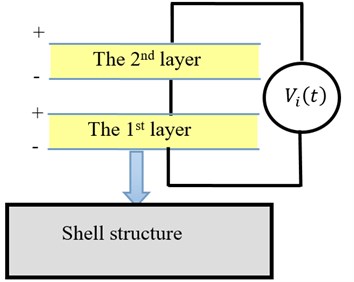
The structure of the harvester is a double curved shallow shell partially covered by several laminated PVDF layers as shown in Fig. 1. The PVDF layers are polarized along the thickness direction and have the same material parameters, which are 1-3 type piezoelectric material. The influence of bonding layers is ignored here in the modeling and the deformation of the shell and PVDF layers are continuous. The vibration of the shell results in deformation of the PVDF layers attached on it, and hence the electrode potential occurs between the electrode pairs due to the piezoelectric effect.
Fig. 1Double-curved shallow shell covered with PVDF layers
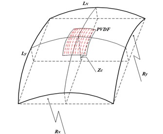
For the shell, it has a rectangle projection on the base plane and its thickness is . The maximum rise of the shell is . The arc lengths of the middle surface are and , respectively. It is assumed that at any point on the mid-surface, the radii of curvature are constant and expressed with and , respectively. , and are used to express the displacements of the mid-surface in , and directions, respectively.
2.2. Dynamic equations of the shell
In this paper, it is assumed that the stiffness and weight of the base structure are much higher than those of the PVDF layers, and hence the influence of PVDF layers on the inertia and stiffness properties of the shell is neglected, which means that the inverse piezoelectric effect is neglected. The dynamic equations of the base shell excited by external forces are established and solved. Thus, the deformation of PVDF layers on the shell is obtained. According to the linear-electroelastic constitutive relation of piezoelectric materials, the voltage on the PVDF layers can then be derived.
For shallow shells, the middle surface strain vector and the curvature vector , allowing for the double curvature, can be expressed as [1]:
The strain vector at the distance from the mid-surface of the shell can be expressed as:
In Eq. (2), , and indicatethe components of the strain, respectively.
The stress-strain relations are as following:
In which, and are the Young’s modulus of the shell and Poisson’s ratio of the shell, respectively., and are the stress components in the base shell.
Based on the thin-shell theory, the kinetic energy and strain energy can be presented as:
The work done by external forces can be given as:
In the expression above, is the density of the shell material. , and are external forces along , and directions, respectively.
Substituting the relationships between strain-displacement and stress-strain into and , then into the Hamilton’s formula:
and integrating it by parts, one can obtain the dynamic equilibrium equations of the double curved shell as following:
The equations above are general for double curved shallow shells with any boundary conditions. For specific boundary conditions, the responses of the shell can be solved by the Galerkin method as long as compatible shape functions are established.
2.3. Open circuit voltages on the PVDF layers
The linear-electroelastic constitutive relation for the PVDF layers is [20]:
where is the stress vector in the PVDF layers; is the strain vector; is the electric field intensity vector; is the elastic stiffness matrix of PVDF materials; is the vector of electric displacement components; is the matrix of piezoelectric constants; is the matrix of permittivity components. Since the d31 type piezoelectric material is adopted, the electric field intensity induced by the direct piezoelectric effect along the thickness direction is presented as [20]:
Then the voltage between the two electrodes introduced by vibration of the shell can be expressed as:
In Eq. (11), is the thickness of each PVDF layers; and are the strains in PVDF layers and can be calculated by Eq. (1) and (2).
When only the thPVDF layer is considered, the voltage can be expressed as:
If all the PVDF layers are connected in series, the total voltage can be calculated according to Eq. (11) and expressed as:
In Eq. (13), the strains and in the top PVDF layer are larger than those in the bottom PVDF layer. So, the farther away from the mid-surface of the shell, the better performance of the PVDF layers in energy harvesting. Moreover, according to Eq. (12) and (13), it can be concluded that the voltage produced by the laminated PVDF layers is about the total summation of the voltage produced by each PVDF layer; the more of the PVDF layers there are, the better the energy harvesting of the system will be.
3. Modal voltage and the characteristics of energy harvesting
To probe the energy harvesting performance of the PVDF layers, a simply supported double curved shallow shell is employed and the expression of open circuit voltage is derived under the modal coordinates system. For different bending modes of the shell, the components of the voltage are explored theoretically.
3.1. Shape function of a double-curved shallow shell
The Galerkin method is adopted to calculate the response of the shell. The displacements of the shell can be approximately expressed as following:
where , , and are modal shape functions of the structure, where and are integers. For a double-curved shallow shell with four edges simply supported, the modal shape functions are as following [21]:
The frequency and response of the shell calculated by the Galerkin method is validated in reference [16].
3.2. Open circuit modal voltage
According to Eq. (11), for PVDF layers located on the area from to and to , the voltage on the thPVDF layer can be derived as:
where is the area of the PVDF layers, , and the strains of the th layer can be expressed as:
In Eqs. (17), is the distance between the mid-surfaces of the shell and the th PVDF layer, and it can be expressed as:
which means that the strain of the mid-surface of the th PVDF layer is employed to express the strain out of the mid-surface. This assumption can be accepted because the thickness of the PVDF is rather small.
Substituting Eq. (18) into Eqs. (17), then into Eq.(16), one can obtain the voltage on the th PVDF layer produced by the vibration of the shell:
If the shell vibrates at the frequency of mode (, ), the components of the modal voltage of the th PVDF layer can be classified as:
where is the voltage introduced by the vibration in the and directions. is the voltage introduced by the membrane strain in the and directions which results from the vibration in the normal direction. is the voltage produced by the bending deformation of the shell.
According to the expressions of the voltage components we derived, it can be obtained that:
(1) The voltages corresponding to the membrane deformation, introduced by the membrane vibrations in the , directions () and the transverse vibration in the normal direction (), are proportional to the thickness of the PVDF layer. The voltage produced by the bending deformation of the shell () is proportional to the square of the thickness of the PVDF layer.
(2) It is important to point out that: according to Eq. (18b), the voltage produced by the membrane stain which is induced by the normal vibration is inversely proportional to the radii curvatures of and . With the increasing of and , the voltage produced by the same magnitude transverse vibration becomes small. When and are close to infinite, the item becomes zero and the total voltage is composed of and . This means that the energy harvesting characteristics of the PVDF layers on curved surfaces are significantly different from that on planar plates. If the PVDF layers are placed on a planar plate, the item disappears, which means that the PVDF layers on shell structures possess better ability in energy harvesting than those used on planar plates.
For a double curved shallow shell, there are following approximate relationships between the radii of the curvature, the respective lengths and the rise of the shell [21]:
So, it can be concluded that with the same respective lengths, the higher the shell rises, the stronger ability to harvest energy the PVDF layers will have.
4. Case study
To verify the analysis and results obtained above, open circuit voltages of the PVDF layers covered on the center area of a simply supported double curved shallow shell is calculated for different cases.
The shallow shell has been used in reference [16]. The geometric and material parameters of the shell are listed in Table 1. The geometric and material parameters of the PVDF layers are listed in Table 2. The respective lengths of the PVDF are 1/4 of the lengths of the shell, which means that the area covered by the PVDF layers is only 1/16 of the total area of the base shell.
Table 1Geometric and material parameters of the shell
Arc length of the shell in direction, (m) | 0.278 |
Arc length of the shell in direction, (m) | 0.247 |
Thickness of the shell, (m) | 0.001 |
Young’s modulus of the shell, (N·m-2) | 70×109 |
Poisson’s ratio of the shell, | 0.33 |
Density of the shell material, (kg·m-3) | 2700 |
Table 2Geometric and material parameters of the PVDF layers
Thickness of the PVDF layer, (m) | 0.0002 |
Length of the PVDF layer in direction, (m) | 0.0695 |
Length of the PVDF layer in direction, (m) | 0.0617 |
Piezoelectric constant of the PVDF, (C/m2) | 0.2 |
Piezoelectric constant of the PVDF, (C/m2) | 0.08 |
Case 1: Change the rise of the shell (), let the ratio increase from 0.001 to 10, then calculate the vibration responses of mode (1, 1) of the shell. The detailed procedure to calculate the system responses is presented in Appendix. Subsequently, strains in the PVDF layer can be obtained, then substituting the strains into Eq. (16), the items of voltages and the total voltage are calculated when only one PVDF layer is adopted and a millimeter displacement is excited at the center of the shell. When 0.001, the shell can be approximated to be a planar plate.
Table 3 shows the magnitudes of the voltages corresponding to the membrane deformation, transverse vibration, bending deformation and the total value expressed in Eq. (15), including the radii of the shell curvature.
Table 3Radii of curvature and magnitudes of the voltages
V/mm | V/mm | V/mm | V/mm | m | m | |
0.001 | –0.4346 | 0.7045 | 52.1451 | 52.1720 | 9661 | 7626 |
1 | –43.4863 | 70.4454 | 79.1050 | 9.6605 | 7.6261 | |
2 | –86.9798 | 140.8907 | 106.0559 | 4.8303 | 3.8131 | |
3 | –130.4921 | 211.3361 | 132.9891 | 3.2202 | 2.5420 | |
4 | –174.0312 | 281.7814 | 159.8954 | 2.4151 | 1.9065 | |
5 | –217.6059 | 352.2268 | 186.7663 | 1.9321 | 1.5252 | |
6 | –261.2252 | 422.6721 | 213.5928 | 1.6101 | 1.2710 | |
7 | –304.8977 | 493.1175 | 240.3663 | 1.3801 | 1.0894 | |
8 | –348.6323 | 563.5628 | 267.0781 | 1.2076 | 0.9533 | |
9 | –392.4375 | 634.0082 | 293.7197 | 1.0734 | 0.8473 | |
10 | –436.3217 | 704.4535 | 320.2827 | 0.9661 | 0.7626 |
Here, it is need to point out that the sign of the is on the contrary of that before and to reflect the phase difference, and the sign before the magnitudes of voltages is included.
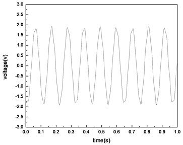
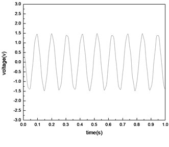
Figs. 2-5 show the variations of , , and with time when 0.001, 2, 5 and 10, respectively. Fig. 6 shows the changing regulation of the voltage magnitudes as listed in Table 3.
Fig. 2Variations of (V~e)mem, (V~e)RxRy, (V~e)bend and (V~e) with time when zc/h= 0.001
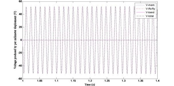
Fig. 3Variations of (V~e)mem, (V~e)RxRy, (V~e)bend and (V~e) with time when zc/h= 2
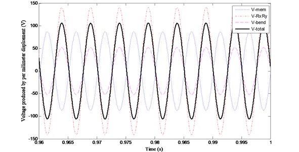
Fig. 4Variations of (V~e)mem, (V~e)RxRy, (V~e)bend and (V~e) with time when zc/h= 5
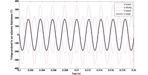
Fig. 5Variations of (V~e)mem, (V~e)RxRy, (V~e)bend and (V~e) with time when zc/h= 10
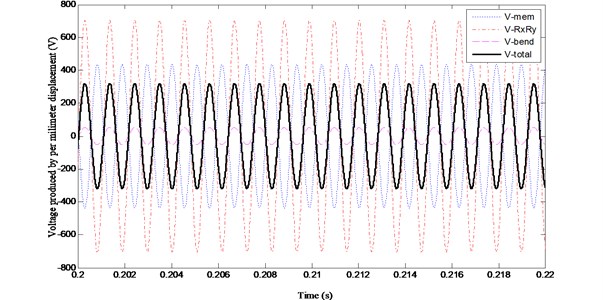
Fig. 6Magnitudes of the voltages produced by per millimeter displacement of the shell with different rises
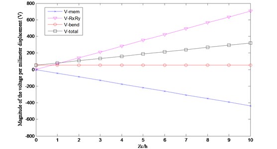
The numerical results indicate that:
(1) With the increasing of the shell’s rise, the radii of the shell decrease significantly, as shown in the 6th and 7th columns in Table 3.
(2) During the vibration of mode (1, 1), and have the same phases. The phase of , is different from the phases of and and the difference between them is 180°. The phase of the total voltage on the PVDF is the same with that of and .
(3) For the planar plate ( 0.001, as shown in Table 3 and Fig. 2), the magnitudes of , and are near zero and the total voltage on the PVDF is determined by , which is introduced by the bending deformation of the shell.
(4) For the shell structure, the magnitudes of , and increase notably with the decreasing of the radii of the shell. But the amplitude of keeps unchanged for shells with different rises, and the value of is the same with that produced on the planar plate.
(5) With the decreasing of the radii, the magnitudes of and , are far greater than that of , and the contribution of to the total voltage becomes smaller. Namely, and , play decisive roles to the total voltage in the shell structures, especially the shells with large curvatures. Furthermore, it can be concluded that at the same vibration level, PVDF layers on the shell structures present stronger ability in energy harvesting than that on planar plates.
Case 2: In the simulations above, only one PVDF layer is covered on the center area of the shell. In this case, two PVDF layers are laminated on the center area of the shell. The magnitudes of voltage items and total voltage are calculated when each of the PVDF layer work alone, as well as the PVDF layers work together. Table 4 lists the numerical results when 10.
Table 4Magnitude of voltages when different PVDF layers work
The 1st PVDF layer works only | The 2nd PVDF layer works only | The 1st and 2nd PVDF layer connected in series | |
V/mm | –436.3217 | –436.3217 | –872.6434 |
V/mm | 704.4535 | 704.4535 | 1408.9070 |
V/mm | 52.1451 | 69.5268 | 121.6719 |
V/mm | 320.2827 | 337.6643 | 657.9470 |
The results indicate that: (1) The magnitudes of and are the same for different PVDF layers, and the magnitude of increases when the distance between the PVDF layer and the mid-surface of the shell increases. This phenomenon agrees well with the deformation regulation of thin shells. (2) When two PVDF layers work together (connected in series), the magnitudes of the voltage items are the summation of the value produced by each layer working alone, which means that laminated PVDF layers are outstanding in energy harvesting than one PVDF layer.
5. Experimental verification
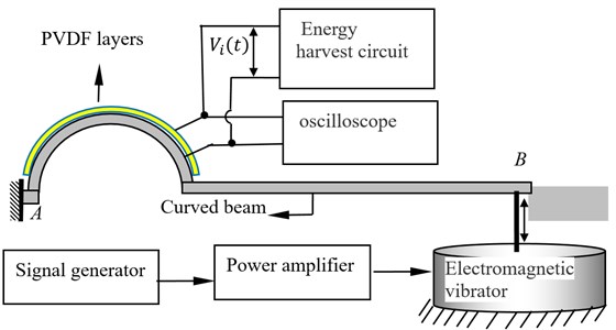
To validate the analysis and results obtained above, energy harvesting experiments are carried out on a straight beam and a curved beam contrastively. PVDF layers with the same dimensions and parameters are bonded on the beams, respectively.
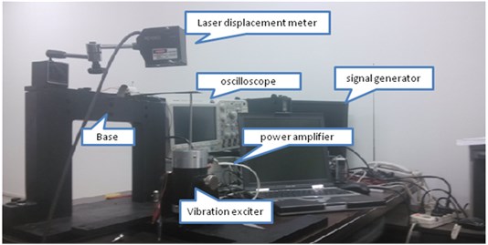
5.1. Experiment system
The beams and PVDF layers used in the experiments are shown in Fig. 7. If the curved section of the curved beam is unbent, it becomes the same with the straight beam shown in Fig. 7. The geometric and material parameters of the beams and PVDF layers are listed in Table 5 and 6.
For the two beams shown in Fig. 7, contrastive experiments are carried out. In the experiments, there are two different types of external excitation.
5.1.1. Excitation 1: base excitation at tip A
In this case, tip A of the beams is fixed on the vibration exciter and tip B is free. The beams undergo sinusoidal excitation at tip A, as shown in Fig. 8(a), in which the curved beam is viewed for instance. The excitation frequency for different beams is their first natural frequencies, respectively.
Fig. 7Photograph of the beams and PVDF layers
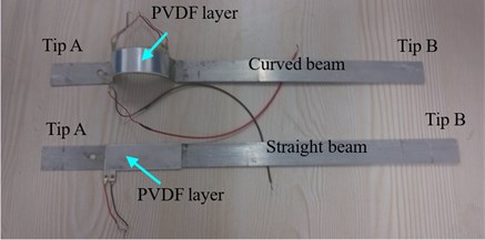
Fig. 8Sinusoidal excitation at the free tip
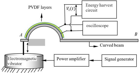
a) Base excitation
b) Excitation 2
Table 5Geometric and material parameters of the curved beam and straight beam
Curved beam | Straight beam | |
Total length of the beam when it spreads(m) | 0.3355 | 0.3355 |
Width of the beam (m) | 0.02 | 0.02 |
Thickness of the beam (m) | 0.001 | 0.001 |
Curvature radius of the curved part (m) | 0.025 | – |
Young’s modulus of the beam (N·m−2) | 70×109 | 70 ×109 |
Poisson’s ratio of the beam | 0.33 | 0.33 |
Density of the shell material, (kg·m−3) | 2700 | 2700 |
Table 6Geometric and material parameters of the PVDF film
Length of the PVDF layer (m) | 0.06 |
Width of the PVDF layer (m) | 0.02 |
Thickness of the PVDF layer (m) | 0.0002 |
Piezoelectric constant of the PVDF, (pC·N−1) | 22-30 |
Piezoelectric constant of the PVDF, (pC·N−1) | 5-6 |
Young’s modulus of the PVDF material (N·m−2) | 2.1×10⁹ |
5.1.2. Excitation 2: sinusoidal excitation at the free tip
In this case, tip A of the beams is fixed on the base and tip B of the beams is free as shown in Fig. 8(b). The sinusoidal excitation is applied at the free end of the beams. The excitation frequency equals to the natural frequency of each beam.
During the experiments, the displacements of the excitation points are controlled to be equal for different beams. In the experiments when the base excitation is applied, the displacement amplitudes of tip A of the two beams are equal. For the clamped beams with sinusoidal excitation, the amplitudes of the free ends are controlled to be equal. The experimental setups for different excitations are shown in Fig. (8). The energy harvesting circuit is shown in Fig. 9.
Under the above excitations, the open circuit voltage response on the PVDF layers are recorded. In addition, the voltage on the PVDF is connected to a storage circuit system as shown in Fig. 9 and the DC voltage on the capacitor is tested as well. The capacitance of the capacitor is 1uF.
Fig. 10 shows the photograph of the curved beam excited at the free end.
Fig. 9Energy harvesting circuit
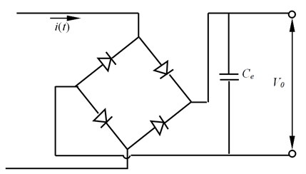
Fig. 10Photograph of the curved beam excited at the free end
5.2. Experimental results
Three groups of experiments are conducted. In group 1, the excitation 1 is adopted and in group 2, the excitation 2 is used. For both groups, only one PVDF layer is partially covered on the straight beam and the curved beam. In group 3, only the curved beam is employed and excitation 1 is considered, but there are two PVDF layers laminated on the curved region. The open circuit voltage on each PVDF layer is tested when the two PVDF layers are in parallel connection and series connection.
5.2.1. Results of group 1
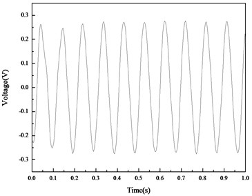
Fig. 11 shows the voltage responses of the PVDF layer on the straight beam when the beam is under the base excitation. The first natural frequency of the beam is 8.75 Hz. The maximum open circuit voltage is 840 mV and the minimum open circuit voltage is –860 mV. Fig. 12 shows the test results of the curved beam. The first natural frequency of the curved beam is 8.25 Hz. The maximum and minimum open circuit voltages are 1400 mV and –1420 mV, respectively. The amplitude of the open circuit voltage introduced by the curved beam is 1.66 times of that introduced by the straight beam, which means that under the same excitation level, the PVDF film on the curved beam presents higher ability in energy harvesting than that on the straight beam.
Fig. 11The voltage responses of the PVDF layer on the straight beam
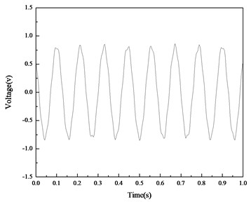
a) Open circuit voltages on the straight beam
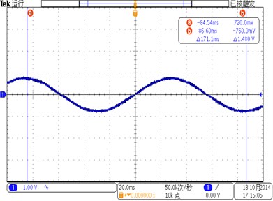
b) Screenshot for the open circuit
Fig. 12The test results of the curved beam
a) Open circuit voltages on the curved beam
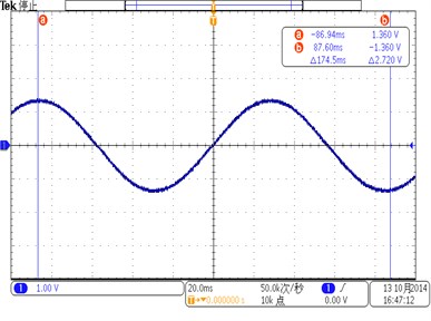
b) Screenshot for the open circuit voltage on the curved beam
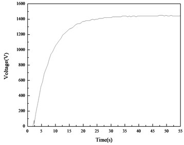
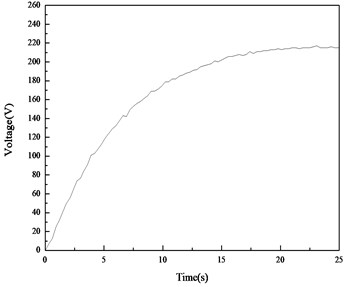
Fig. 13 and Fig. 14 show the DC voltage on the capacitor during the energy harvesting for the straight beam and curved beam, respectively. It can be seen that during the capacitor charging process, the slope of the charging curve for the curved beam is much larger than that for the straight beam. According to the test curve, the rate of energy harvesting on the curved beam is about 62.5 mV/s, and that on the straight beam is 25 mV/s. The saturation voltage for the curved beam and straight beam is about 1450 mV and 690 mV, respectively.
The results of this group of experiments show that the energy harvesting ability of the PVDF layer on the curved beam is much higher than that on the straight beam.
Fig. 13DC voltages on the capacitor for the straight beam
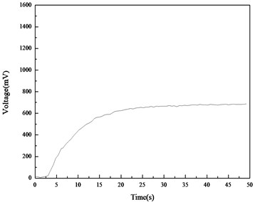
Fig. 14DC voltages on the capacitor for the curved beam
5.2.2. Results of group 2
In this group of experiments, the straight beam and curved beam are clamped at end A respectively and are disturbed at their free end with the same displacements, respectively, as shown in Fig. 8(b). The open circuit voltages on the PVDF layers of the two different beams are tested, together with the DC voltages on the capacitor during the energy harvesting.
Fig. 15Open circuit voltages on the straight beam
a) Test date
b) Data smoothed
Fig. 16Open circuit voltages on the curved beam
a) Test date
b) Data smoothed
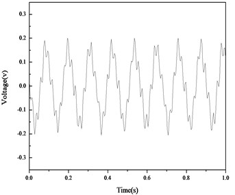
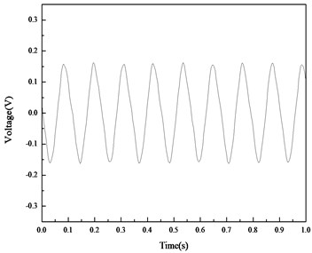
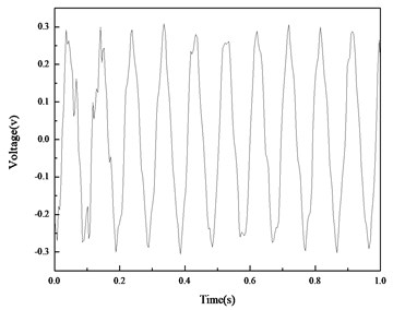
Fig. 15 and 16 show the open circuit voltages. Fig. 17 and 18 give the DC voltages on the capacitor for the two beams. The frequency for the straight beam and curved beam are 8.87 Hz and 10.40 Hz, respectively.
Figs. 14-15 show that under the same disturbance at the free end, the amplitude of open circuit voltage for the straight beam is about 163 mV and that for the curved beam is about 280 mV. The amplitude of the open voltage produced on the curved beam is 1.72 times of that on the straight beam. The results in Fig. 17 and 18 show that the rate of energy harvesting on the curved beam is much higher than that on the straight beam, which is consistent with the conclusion in the experiments of group 1.
Fig. 17DC voltage on the capacitor for the straight beam
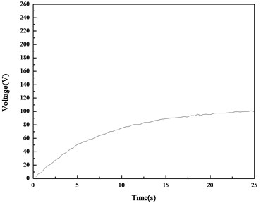
Fig. 18DC voltage on the capacitor for the curved beam
5.2.3. Results of group 3
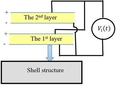
In the experiments of group 3, only the curved beam is employed to harvest energy and the beam is under the base excitation as shown in Fig. 8(a). There are two PVDF layers laminated on the curved part of the beam. The circuit voltages on the 1st layer (near the shell) and the 2nd layer are tested, including the voltages when the two PVDF layers are in parallel connection and series connection, respectively. It is necessary to point out that for all the tests in group 3, the excitation keeps the same.
Fig. 19 shows the open circuit voltages on the bottom PVDF, and the voltages on the top layer are shown in Fig. 20.
Fig. 19Open circuit voltages on the 1st PVDF layer
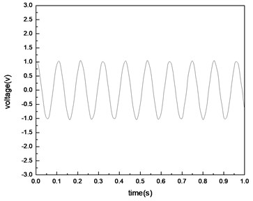
Fig. 20Open circuit voltages on the 2nd PVDF layer
It can be seen that with the same base excitation, the voltage on the top layer is larger than that on the bottom layer, this agrees well with the conclusions obtained from the theory model.
Fig. 21 shows the open circuit voltage responses when the two PVDF layers are connected in series. The voltage responses for the parallel connection are shown in Fig. 22. The schematic diagrams for the series connection and parallel connection are shown in Fig. 23.
Fig. 21Open circuit voltages for series connection
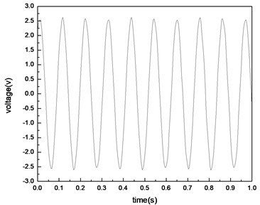
Fig. 22Open circuit voltages for parallel connection
Results in Fig. 21 and 22 show that: (1) The amplitude of the open circuit voltage when the two PVDF layers are in series connection is a little less than the summation of the amplitudes when they work alone, but it is much higher than that when only one PVDF layer is employed. (2) The amplitude of the open circuit voltage when the two PVDF layers are in parallel connection is less than that in series connection and it is even less than the amplitude when the 2nd layer is used alone.
Fig. 23Schematic diagram for circuit
a) In series connection
b) In parallel connection
The conclusions obtained from group 3 are consistent with that obtained from the simulations. Moreover, it makes it clear that the connection of several PVDF layers in series mode can improve the energy harvesting efficiency significantly.
6. Conclusions
In this study, energy harvesting characteristics of PVDF layers laminated on double curved shallow shells are investigated numerically and experimentally. Analytical expressions of the open circuit voltages for PVDF layers on double curved shallow shells are derived. Energy harvesting experiments on a straight beam and a curved beam are carried out. Theoretical analysis and experimental results show that:
1) PVDF layers covered on curved shells possess higher energy harvesting ability than that covered on planar plates. The smaller the radii of the shell are; the higher open circuit voltage will be introduced on the PVDF layers.
2) The open circuit voltage introduced by the transverse vibration of the shell plays a decisive role in the total voltage on the PVDF layer. But for a planar plate, this item equals to zero and the total voltage is mainly determined by the bending deformation.
3) When several PVDF layers are laminated on the shell surface and connected in series, the magnitude of the total voltage approximately equals to the summation of the voltages produced by each layer working alone, which means that laminated PVDF layers have advantages over a single PVDF layer in energy harvesting.
4) In this work, the laminated PVDF layers covered on the center area of the base shell and only (1, 1) mode is considered in the analysis. For the vibration of (1, 1) mode, the optimal position for the PVDF layers is the center of the shell, but for the vibrations of other modes, the center position is not the best choice for the PVDF layers. So, the location optimization for the PVDF layers is the subsequent work to be done. Moreover, for a broadband vibration, employing distributed PVDF layers to improve the energy harvesting ability is also to be considered.
References
-
Anton S. R., Sodano H. A. A review of power harvesting using piezoelectric materials. Smart Materials and Structures, Vol. 16, 2007, p. 1-21.
-
Kim H. S., Kim J. H., Kim J. A review of piezoelectric energy harvesting based on vibration. International Journal of Precision Engineering and Manufacturing, Vol. 12, 2011, p. 1129-1141.
-
Saadon S., Sidek O. A review of vibration-based MEMS piezoelectric energy harvesters. Energy Conversion and Management, Vol. 52, 2011, p. 500-504.
-
Erturk A., Inman D. J. An experimentally validated bimorph cantilever model for piezoelectric energy harvesting from base excitations. Smart Materials and Structures, Vol. 18, Issue 2, 2009, p. 025009.
-
Bilgen O., Wang Y., Inman D. J. Electromechanical comparison of cantilevered beams with multifunctional piezoceramic devices. Mechanical Systems and Signal Processing, Vol. 27, 2012, p. 763-777.
-
Rastegar J., Pereira C., Nguyen H. L. Piezoelectric-based power sources for harvesting energy from platforms with low frequency vibration. Proceedings of Smart Structures and Materials Conference, 2006, p. 617101.
-
Roundy S., Wright P. K. A piezoelectric vibration based generator for wireless electronics. Smart Materials and Structures, Vol. 13, Issue 5, 2004, p. 1131.
-
Zhou L., Sun J., Zheng X. J., Deng S. F., Zhao J. H., Peng S. T., Zhang Y., Wang X. Y., Cheng H. B. A model for the energy harvesting performance of shear mode piezoelectric cantilever. Sensors and Actuators A, Vol. 179, 2012, p. 185-192.
-
Bonello P., Rafiqueand S., Shuttleworth R. A theoretical study of a smart electromechanical tuned mass damper beam device. Smart Material Structures, Vol. 21, 2012, p. 125004.
-
Junior C. D. M., Erturk A., Inman D. J. An electromechanical finite element model for piezoelectric energy harvester plates. Journal of Sound and Vibration, Vol. 327, 2009, p. 9-25.
-
Chen X., Yang T., Wang W., Yao X. Vibration energy harvesting with a clamped piezoelectric circular diaphragm. Ceramics International, Vol. 38, 2012, p. 271-274.
-
Xie X. D., Wang Q., Wu N. Energy harvesting from transverse ocean waves by a piezoelectric plate. International Journal of Engineering Science Vol. 81, 2014, p. 41-48.
-
Zhang Y. H., Niu H. P., Xie S. L., Zhang X. N. Numerical and experimental investigation of active vibration control in cylindrical shells partially covered by laminated PVDF actuator. Smart Materials and Structures Vol. 17, Issue 3, 2008, p. 35024.
-
Zhang Y. H., Zhang X. N., Xie S. L. Adaptive vibration control of cylindrical shell with laminated PVDF actuator. Acta Mechanica, Vol. 210, 2010, p. 85-98.
-
Zhang Y. H., Zhang X. N., Elliott S. J. Numerical and experimental investigations of actuating characteristics of laminated polyvinylidene fluoride actuator used on paraboloidal shells. Journal of Sound and Vibration, Vol. 331, 2012, p. 510-521.
-
Zhang Y. H., Elliott S. J., Zhang X. N., Nourzad D. J. Active vibration control of a double-curved shell with a laminated polyvinylidene fluoride actuator. International Journal of Aerospace and Lightweight Structures, Vol. 2, Issue 2, 2002, p. 199-219.
-
Yoon H. S., Washington G., Danak A. Modeling, optimization, and design of efficient initially curved piezoceramic unimorphs for energy harvesting applications. Journal of Intelligent Material Systems and Structures, Vol. 16, Issue 10, 2005, p. 877-888.
-
Mossi K., Green C., Ounaies Z., Hughes E. Harvesting energy using a thin unimorph prestressed bender, geometrical effects. Journal of Intelligent Material Systems and Structures Vol. 16, 2005, p. 249-261.
-
Huang S. L., Chu C. C., Chang C. C., Tzou H. S. Electromechanical coupling and signal distribution of a circular cylindrical shell coupled with segmented sensors. Proceedings of IMECE2008-68016, Boston, Massachusetts, USA, 2008.
-
Tzou H. S. Piezoelectric Shells. Kluwer Academic Publishers, Boston, MA/Dordrecht, 1993, p. 13-48.
-
Warburton G. B. The Dynamic Behaviour of Structures, Pergamon Press, UK, Chapter 5, 1976
About this article

The financial support from the National Natural Science Foundation of China (Grant No. 11302160) and NSAF (Grant No. U1630120) are gratefully acknowledged.
