Abstract
Z-source converters have been used in new energy sources because of their advantages. These converters have attracted considerable attention under high-frequency conditions given their high power density and high conversion efficiency. However, the stability of a system of ultra-high frequency Z-source converters are likely to be affected because of the inappropriate selection of parameters or the interference of weak signals in the process of the system. These factors will render such converters unable to work properly. The chaotic bifurcation behavior of Z-source converters based on peak current control mode is analyzed in this study. A precise discrete iterative mapping model for such converters is established, and the regional stability of a system is determined based on the characteristic value of changes in the Jacobian matrix. Finally, the bifurcation and chaos phenomena in a high-frequency Z-source converter and the accuracy of the aforementioned analysis are verified via experiments. The conclusion drawn from this study does not only can provide a reference for the stable operation of ultra-high frequency Z-source converters, but also presents a theoretical basis for optimizing system parameters and improving control performance.
1. Introduction
A power converter is a strongly nonlinear control system. The opening and closing of cycles under different topologies are achieved by turning the switch tube on or off, which can easily cause the nonlinear behavior of switching converters. Period doubling bifurcation, boundary collision bifurcation and chaos, and other nonlinear phenomena [1-3] in DC/DC converters [4, 5], DC/AC inverters [6], and power factor correction converters [7] are common nonlinear behavior. When a power converter works in a chaotic region, the stable running state of a system will be changed, and its control performance will be considerably affected. The ripple of the voltage will enlarge, which is a serious situation, and the converter will be unable to work properly.
At present, research on the field of power electronics mainly focuses on the discovery and analysis of bifurcation, chaos, and other nonlinear behavior [8-10]. Research shows that the nonlinear behavior of a boost converter is controlled via digital current mode based on simulation and experimental results. The stability of a converter was analyzed by Amit Kumar Singha et al. [11]. The bifurcation phenomenon of a buck converter under current mode control was discussed, and experimental verification was performed by Biswarup Basak [12]. The chaotic bifurcation behavior of a flyback converter with peak current mode control was introduced, and the influences of different bifurcation parameters on the chaotic phenomenon were analyzed via an iterative mapping model [13].
To date, the research points for high-frequency Z-source converters [14, 15] have mainly focused on performance improvement, topology derivation and practical engineering applications [16]. The power factor correction of a Z-source converter is introduced and then it is applied to an electric vehicle battery charging system, which increased the stability of the system. A novel circuit topology and control strategy for a voltage source inverter based on a quasi-Z-source inverter was proposed by Hu Ruizhe [17]. The stability analysis of a system, particularly the introduction of nonlinear behavior, is currently extremely rare. The current study starts from the DC link of an ultra-high frequency Z-source converter and adopts peak current control mode. A discrete iterative mapping model for continuous current mode is then established based on the equation of state. The bifurcation diagram of the system shows that period doubling bifurcation and the effect of reference current size on the stability of the system are determined via the characteristic value of the Jacobian matrix. The occurrence of a nonlinear phenomenon is confirmed via circuit simulation. Finally, the accuracy of the theoretical analysis is verified using the experimental data.
2. Working principle of and model for ultra-high frequency Z-source converter
2.1. Working principle of ultra-high frequency Z-source converter
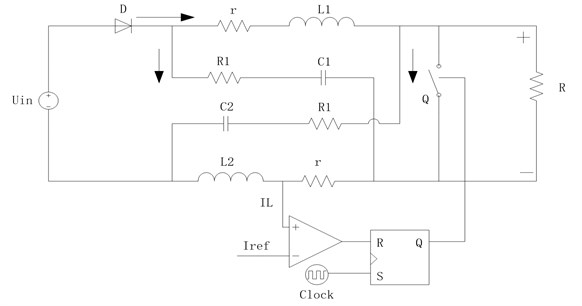
The main structure of an ultra-high frequency Z-source converter comprises a diode D and an impedance network that is connected between the DC voltage source and the conventional voltage source converter. The converter impedance network contains two identical inductors and two identical capacitors, which are arranged to form an X-type structure. Fig. 1 illustrates the circuit diagram of the Z-source converter under peak current mode control. This system mainly involves a clock signal that controls the turning on of the switch. This clock signal also sets the RS flip-flop to 1 at regular intervals. The switch is turn off at 0, and the inductor current increases until the required is reached. Afterward, the inductor inverts the output signal at 1. Peak current mode control exhibits good stability and improved noise elimination. It does not require harmonic compensation, and is simple and convenient to achieve. Moreover, this control mode can limit peak current in the circuit, thereby protecting the device. Consequently, a wide range of applications are obtained. Peak current mode control is the most widely used current mode control method.
Fig. 1Schematic of an ultra-high frequency Z-source converter based on peak current mode control
2.2. Dynamic model for ultra-high frequency Z-source converter
The operation principle of an ultra-high frequency Z-source converter is based on peak current control mode according to the working state of straight switch and diode . In continuous current mode, two types of working conditions can be achieved, and the circuit is switched periodically between the two modes of operation, as shown in Fig. 2.
Fig. 2DC-link equivalent circuit of the ultra-high frequency Z-source converter
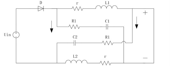
a) Equivalent circuit under shoot-through mode
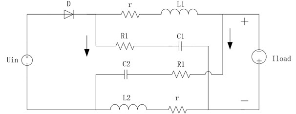
b) Equivalent circuit under non-shoot-through mode
In working mode 1, the shoot-through state is represented as on and off. The state equation is written as follows:
In working mode 2, the non-shoot-through state is represented as off and on. The state equation is expressed as follows:
We assume that is the inductance of the Z-source network, is the capacitance of the Z-source network, is the inductor current of the Z-source network, is the capacitance voltage of the Z-source network, is the parasitic resistor of the inductor, is the series resistance of capacitance, is the load resistance, and is the output voltage.
We calculate the discrete iterative model of the system using the stroboscopic mapping method based on Eqs. (1) and (2). is the duty cycle of the nth period , , , and the discrete iterative equations can be expressed as . The state equation derived from Eq. (1) and Eq. (2) is specified as Eq. (3) and Eq. (4), respectively:
where the state vector is defined as:
For the discrete model in the stroboscopic map, the equation is expressed as follows:
The equation of state of the system is Eqs. (3) and (4), whereas the discrete model for the system in the th cycle can be obtained as:
where , and .
When cycle is smaller, the method of approximate discretization [18] is used in this study. As a result the integral terms of these equations can be simplified and expressed as follows:
Eq. (8) can be substituted into Eq. (9) and expressed as discrete mapping Eq. (10) as follows:
The switching function can be derived as follows:
], the state of the converter is altered.
3. Parameter design of ultra-high frequency Z-source network
An ultra-high frequency Z-source converter has certain properties that are not found in traditional converters because of the added unique Z-source impedance network, and thus, the parameter design of an ultra-high frequency Z-source converter is particularly important. The design is related to the performance of the entire system. It also has a critical effect on our subsequent analysis.
Combined with the system requirements, the parameters of the system are listed in Table 1.
Table 1System parameters
Switching cycle | 1 µs | Through cycle | 0.4 µs | ||
Capacitance voltage | 240 V | Duty ratio | 0.4 | ||
Inductor current | 1 A | Load resistance | 20 Ω |
3.1. Design of network capacitor of converter
The quality of the capacitor voltage of an ultra-high frequency Z-source converter directly affects the quality of the voltage of the input DC link of the converter, which consequently determines the quality of the output voltage. The higher the Z-source capacitance value, the higher the system stability will be. However, the cost of the capacitor will be increased from the design point of view. To comprehensively consider various factors and to satisfy the requirements of analysis, the ultra-high frequency Z-source converter network parameters of the capacitor value are determined in this study.
When the system works under a non-straight state, the ultra-high frequency Z-source capacitor is charged. The capacitance voltage value at this point is gradually increased. The current value of the capacitance of the Z-source converter is:
When the system works under a straight state, the ultra-high frequency Z-source capacitor discharge is inductive charging, and the current on the capacitor is the same as the inductor current. The Z-source capacitance current at this point is:
The research object in this study is the ultra-high frequency Z-source converter, and thus, switching frequency is sufficiently high. The value of the inductor current can be approximated as a constant value as follows:
Fig. 3Ultra-high frequency Z-source capacitance voltage waveform
On the basis of the opening and closing of the switch tube, the ultra-high frequency Z-source capacitor voltage waveform can be obtained from Fig. 3. When Eqs. (13, 14) are combined, then this waveform can also be obtained from Fig. 3:
From the data, should be less than 3 % , where , . The equivalent series resistance of the inductance and capacitance of the Z-source network are disregarded, then can be deduced from state space averaging equation [19]:
From Eqs. (13) to (16), the following equation can be obtained:
The aforementioned parameters are integrated into Eq. (17):
3.2. Design of inductor in converter network
The inductance value of the ultra-high frequency Z-source network is as important as the capacitance value. The design of the inductor also affects the working status of the system. The ripple of the inductor current is related to the inductance value. The higher the inductance value, the smaller the ripple of the inductor, and the more stable the system will be. However, an increase in volume is followed by an increase in cost. Therefore, the design should comprehensively consider various factors. The inductance value is designed to fulfill the requirements of the system based on the analysis of the ripple.
The Z-source inductance voltage is a switching pulse under a steady state condition. The inductor is charged, and the inductor current increases under shoot-through state. The inductor voltage is during this period. The inductor is discharged, and the inductor current is reduced under non-shoot-through state. The inductor voltage is , as shown in Fig. 4.
Fig. 4Ultra-high frequency Z-source inductor current and voltage waveform
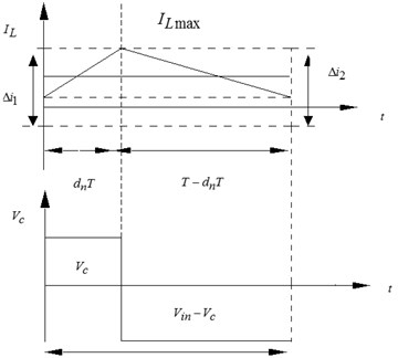
In a switching cycle, when , the circuit is shown in Fig. 2(a):
where is the ultra-high frequency Z-source inductor voltage under through state, and is the ultra-high frequency Z-source inductor current increment under through state.
When , the circuit is shown in Fig. 2(b):
where is the inductive voltage of the ultra-high frequency Z-source converter under non-straight through state, and is the inductance current increment of the ultra-high frequency Z-source converter under non-straight through state.
The steady state is known, and thus, the following can be obtained in a switching cycle:
Eqs. (18) to (20) can be expressed as:
Then, the following can be obtained:
The maximum allowable value of the amplitude of the harmonic current is . The inductance value of the ultra-high frequency Z-source converter is satisfied as follows:
In addition to the aforementioned requirements, the resonant frequency of the capacitor in the case of non-resonance is:
If the design requirement of the ultra-high frequency Z-source network does not produce resonance, then the switching frequency of the converter must not be higher than the resonant frequency of the Z-source network in this study, i.e.:
The inductance value can be obtained as follows:
When the two preceding aspects are integrated, the value of the ultra-high frequency Z-source converter inductor is:
From the design requirements, is known. The circuit parameters in Table 1 are introduced into Eq. (27), which can derive:
Fig. 5Nonlinear typical waveform of the ultra-high frequency Z-source converter under peak current control
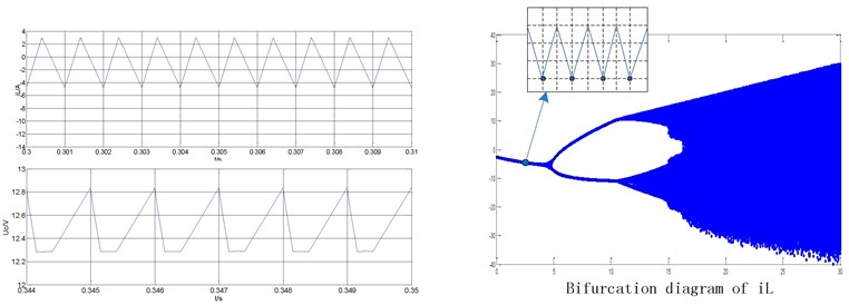
a) Typical waveforms of period-1 state ( 3 A)
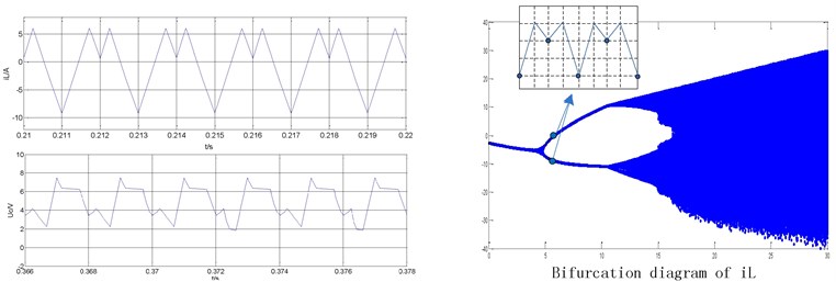
b) Typical waveforms of period-2 state ( 6 A)
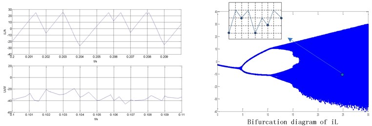
c) Typical waveforms of chaotic state ( 25 A)
4. Dynamic behavior analysis of ultra-high frequency Z-source converter
4.1. Nonlinear phenomenon of converter
To more directly reflect the nonlinear phenomenon of the system, the simulation module of an ultra-high frequency Z-source converter with peak current control mode is established using the state space analysis method based on MATLAB. The simulation values of the Z-source network inductor current and capacitor voltage are shown on the left of the figures.
Fig. 5 illustrates the time domain waveform of the inductor current of the ultra-high frequency Z-source converter under different reference current conditions. Fig. 5(a) shows the reference current 3 A. The figure indicates that the system works under period-1 state. The simulation results on the left show that is the capacitance voltage and is the inductor current of the Z-source network. The bifurcation diagram of is presented on the right. Fig. 5(b) shows the reference current 6 A. The system can work under period-2 state. Fig. 5(c) shows the reference current 25 A. The system is known to be under a state of chaos.
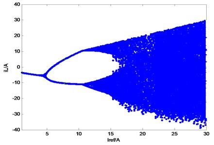
When the input voltage of the converter is set as 80 V, 0.5 mH, 0.013 μf, 0.5 Ω, 0.02 Ω, 18 Ω, –1, 2-30 A, and 1 MHz. The output current reference value is selected as the analysis variable, and the bifurcation diagram is drawn as shown in Fig. 6.
Fig. 6Inductance current bifurcation diagram with reference current Iref as the bifurcation parameter
4.2. Converter stability analysis
From the preceding discussion, the variation of the reference current parameter or the external disturbance will change the stable operation of the system, and thus, produce the bifurcation and chaos phenomena. The Jacobian matrix is an effective tool for analyzing stability. In this study, we use the Jacobian matrix to analyze the stability of the fixed point of the converter and the characteristics of the local bifurcation. The Jacobian matrix of the fixed point is established in the beginning.
We assume that the controlled system is stable under a single period state, and that the input voltage and reference voltage always remain unchanged. , , and are set as the periodic solutions for a steady state. The perturbation and linearization [20, 21] of Eq. (5) can then be expressed as follows:
At , the following can be obtained:
Consequently, the following can be obtained:
Eq. (30) can be substituted into Eq. (28) to yield Eq. (31):
We can obtain the Jacobian matrix as follows:
where:
Before the eigenvalues of the Jacobian matrix of the system is calculated, the steady state periodic solutions and of the discrete mapping equations of the controlled ultra-high frequency Z-source converter system are first determined. The equilibrium point of the discrete mapping equation of the system is the single period steady state solution for the system.
Let , and . Through Eqs. (8) and (9), the following can be obtained:
Eqs. (33) and (34) are then derived as:
Simultaneously, the switching function satisfies:
The schematic of the peak current control of the ultra-high frequency Z-source converter is shown in Fig. 1. On the basis of the aforementioned parameters, the characteristic value of the Jacobian matrix is calculated with reference current as the bifurcation parameter. When 3.5 A, the steady state periodic solution is obtained via numerical calculation:
The system is stable given that 1 and 1 at reference current 3.5 A. When , the system is under a single period steady state. As shown in Fig. 7, all the characteristic values of the Jacobian matrix of the ultra-high frequency Z-source converter lie on the real axis of the coordinate axes and the change of is faster than that of . The change of is extremely slow. The system becomes unstable as long as a characteristic value exists over the unit circle. The maximum is selected as the basis to study the stability of the system. When the value of is between 4.8 and 4.9, will be larger than 1. Then, the system will enter an unstable state from a stable operation.
Fig. 7Motion change trend of the Jacobian matrix eigenvalue
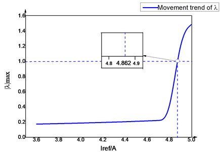
To determine the critical value of , the variations of the eigenvalues of the Jacobian matrix are listed when 4-5 A in Table 2.
Table 2Eigenvalues of the different values of the reference current Iref for peak current mode control
Iref | System state | |||
4.5 | 0.6294 | 0.2161 | −0.4071 | Stable |
4.6 | 0.6245 | 0.2220 | −0.3801 | Stable |
4.7 | 0.6196 | 0.2282 | 0.3546 | Stable |
4.8 | 0.6148 | 0.2349 | −0.3306 | Stable |
4.9 | 0.1058 | 1.3586 | 0.0004 | Bifurcation |
5.0 | 0.1130 | 1.4873 | 0.0005 | Unstable |
As shown in Table 2, when 4.9 A, the value of is close to 1. 4.862 A, –1.2241 and –0.0004 can be calculated through a large number of numerical calculations. The value of at this time is the critical value of system instability. If the value of exceeds this value, then the system will enter bifurcation. When the value of is less than 4.862 A, then the eigenvalues of the Jacobian matrix of the system at fixed points are less than 1. The fixed point is a stable node at this instance. When the value of is higher than 4.862 A, the system is exposed to period doubling bifurcation. The original fixed point of the system of period 1 is unstable at this instance. Instead, two stable solutions are available for period 2. The situation is illustrated in Fig. 6.
The Jacobian matrix method is used to judge stability. This method can be applied to accurately analyze and identify the location of the bifurcation point. The bifurcation point is determined using this method in practical applications, and then the parameters of the converter are designed. Finally, to ensure that the system will work in a stable running area, the influence of the circuit parameters on the stability of the fixed point and the system are discussed as follows. The different values of reference current are selected as the bases in this study. The effects of the inductance and capacitance of the Z-source network on system stability is analyzed. The corresponding fixed point stability boundary curves are illustrated in Fig. 8. From Fig. 8(a), a conclusion can be drawn that the area below the curve is unstable. With the increase in the reference current , the unstable region of the fixed point of capacitor will continue to increase. As shown in Fig. 8(b), the region below the curve is stable. With the increase in the reference current , the stability region of the fixed point of inductance L becomes smaller. Fig. 8(c) illustrates the stability of the three parameter domains using the Jacobian matrix method.
Fig. 8Stability region boundary curves under different parameter variations
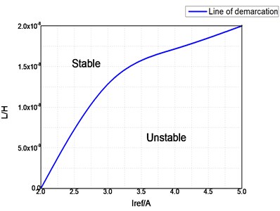
a) Influence of inductance parameters on the stability region
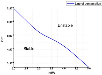
b) Influence of capacitor parameters on the stability region
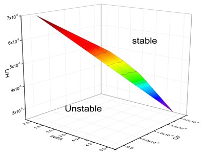
c) Distribution map of the stable region of the three parameters of the Jacobian matrix method
5. Experiment verification
To verify the accuracy of the theoretical analysis and the simulation of the converter circuit, a relevant circuit verification analysis is conducted. The circuit model of the ultra-high frequency Z-source DC/DC converter based on peak current control mode is built based on the aforementioned parameters. The experimental circuit is consistent with the simulation model. A KLP250 isolation drive chip is applied in the drive circuit. The parameters of the given circuit are as follows: input voltage 80 V, 1 MHz, load resistance 18 Ω, capacitance resistance 0.5 Ω, inductance resistance 0.02 Ω, ultra-high frequency Z-source network inductance 0.5 mH and network capacitance 0.013 μf.
The reference current changes from 2 A to 20 A under the driving signal of the switch tube and the clock signal in the cycle. The experimental waveforms of the inductor current and the capacitor voltage of the Z-source network are shown in Fig. 9. Channels one and two show the value of the inductor current and the capacitor voltage under period 1, period 2, and chaotic states. Fig. 9(a) shows a stable waveform under period-1 state at reference current 3 A. Fig. 9(b) shows the waveform under period-2 state at reference current 6 A. Fig. 9(c) shows that the system enter a chaotic state at reference current 25 A.
Fig. 9Experimental waveforms of the inductor current and capacitor voltage under different reference currents
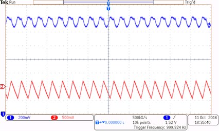
a)3 A (Typical waveforms under period-1 state)
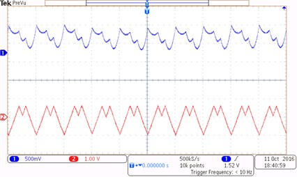
b) 6 A (Typical waveforms under period-2 state)
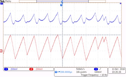
c) 25 A (Typical waveforms under a chaotic state)
The experimental results indicate that the experimental waveforms are in full compliance with the simulation model results of the circuit at the critical point of the reference current. The bifurcation diagram is consistent with the model based on the discrete iterative map equation model. The accuracy of the theoretical analysis is verified. In summary, the ultra-high frequency DC/DC Z-source converter under different reference currents will exhibit a nonlinear behavior.
6. Conclusions
In view of the nonlinear characteristics of power electronic converters in application processes, the nonlinear dynamic behavior of an ultra-high frequency Z source converter under peak current control is investigated in this study. A discrete iterative mapping model is established based on the equation of state of the converter for the analysis and drawing of the bifurcation diagram of the Z-source converter when different parameters are given. The stability of the converter is analyzed using the trajectory of the eigenvalues of the Jacobian matrix. Moreover, the stable operating region is determined based on the parameters of the Z-source inductance, capacitance, and reference current at an ultra-high frequency. The accuracy of the theoretical analysis is verified via the experimental results. The findings of this study can provide references for analyzing the nonlinear mechanism of this type of converter. Moreover, this study provides important theoretical guidance for the optimal design and control of converter parameters.
References
-
Roghayeh Gavagsaz-Ghoachani, Phattanasak Matheepot, Martin Jean-Philiooe Generalization of an averaged model approach to estimate the period-doubling bifurcation onset in power converters. IET Power Electronics, Vol. 9, Issue 5, 2016, p. 977-988.
-
Parvathyshankar Deivasundari, Govindarajan Vma, Rengasamy Poovehi Analysis and experimental verification of Hopf bifurcation in a solar photovoltaic powered hysteresis current-controlled cascaded-boost converter. IET Power Electronics, Vol. 6, Issue 4, 2013, p. 763-773.
-
Xie Fan, Zhang Bo, Yang Ru, Herbert Ho-Ching Iu Detecting bifurcation types and characterizing stability in DC-DC switching converters by duplicate symbolic sequence and weight complexity. IEEE Transactions on Industrial Electronics, Vol. 60, Issue 8, 2013, p. 3145-3156.
-
Parvathyshankar Deivasundari, Govindarajan Uma, Christy Vincen, Krishnamurthy Murali Non-linear intermittent instabilities and their control in an interleaved DC/DC converter. IET Power Electronics, Vol. 7, Issue 5, 2014, p. 1235-1245.
-
Deivasundari P., Uma G., Poovizhi R. Analysis and experimental verification of Hopf bifurcation in a solar photovoltaic powered hysteresis current-controlled cascaded-boost converter. IET Power Electronics, Vol. 6, Issue 4, 2013, p. 763-773.
-
Hsieh Fei-Hu, Wang Hen-Kung, Chang Po-Lun, Wu Hsuan-Chiang Nonlinear dynamic behaviors in voltage-mode controlled single-phase half-bridge inverters via varying proportional gain. International Conference on Machine Learning and Cybernetics, 2011, p. 1274-1278.
-
Orabi M., Ninomiya T. Nonlinear dynamics of power-factor-correction converter. IEEE Transactions on Industrial Electronics, Vol. 50, Issue 6, 2003, p. 1116-1125.
-
Wan Cheng, Huang Meng, Tse C. K. Nonlinear behavior and instability in a Three-phase boost rectifier connected to a non-ideal power grid with an interacting load. IEEE Transactions on Power Electronics, Vol. 28, Issue 7, 2013, p. 3255-3265.
-
Morcillo Jose D., Burbano Daniel, Angulo Fabiola Adaptive ramp technique for controlling chaos and subharmonic oscillations in DC-DC power converters. IEEE Transactions on Power Electronics, Vol. 31, Issue 7, 2016, p. 5330-5343.
-
Tse C. K., Bemardo M. Di Complex behavior in switching power converters. Proceeding of IEEE, Vol. 90, Issue 5, 2002, p. 768-781.
-
Amit Kumar Singha, Santanu Kapat, Soumitro Banerjee, Jayanta Pal Nonlinear analysis of discretization effects in a digital current mode controlled boost converter. IEEE Journal on Emerging and Selected Topics in Circuits and Systems, Vol. 5, Issue 3, 2015, p. 336-344.
-
Biswarup Basak, Sukanya Parui Exploration of bifurcation and chaos in Buck converter supplied from a rectifier. IEEE Transactions on Power Electronics, Vol. 25, Issue 6, 2010, p. 1556-1564.
-
Arnab Ghosh, Subrata Banerjee, Saptarshi Basak, Chandan Chakraborty A study of chaos and bifurcation of a current mode controlled flyback converter. Industrial Electronics, 2014, p. 392-397.
-
Cao Dong, Jiang Shuai, Yu Xianhao, Peng Fangzheng Low-cost semi-Z-source Inverter for single-phase photovoltaic systems. IEEE Transactions on Power Electronics, Vol. 26, Issue 12, 2011, p. 3514-3523.
-
Galigekere Veda Prakash, Kazimierczuk Marian K. Analysis of PWM Z-source DC-DC converter in CCM for steady state. IEEE Transaction on Circuit and Systems I: Regular Papers, Vol. 59, Issue 4, 2012, p. 854-863.
-
Nomar S. González-Santini, Hulong Zeng, Yaodong Yu, Fang Zheng Peng Z-source resonant converter with power factor correction for wireless power transfer applications. IEEE Transactions on Power Electronics, Vol. 31, Issue 11, 2016, p. 7691-7700.
-
Hu Ruizhe, Chen Daolian, Xu Zhilong Novel single-phase voltage type quasi Z source inverter. Transactions of China Electrotechnical Society, Vol. 30, Issue 16, 2015, p. 33-41.
-
Lu Weiguo, Zhou Luowei, Luo Quanming, Du Xiong Chaos control and optimization of boost converter with delayed feedback. Journal of Physics, Vol. 11, Issue 56, 2007, p. 6275-6280.
-
Chen Yicheng Design of Single Phase Photovoltaic Grid Connected Inverter Based on Z-Source Network 400W, Shanghai Jiao Tong University, Shanghai, 2014.
-
Villalva M. G., De Siqueira T. G., Ruppert E. Voltage regulation of photovoltaic arrays: small-signal analysis and control design. IET Power Electronics, Vol. 3, Issue 6, 2010, p. 869-880.
-
Chen Yan, Zheng Yong Nonlinear behavior analysis of Z-source DC/DC converter based on current control. Journal of Vibroengineering, Vol. 15, Issue 3, 2013, p. 1576-1584.
About this article

This study is supported by the National Natural Science Foundation of China (Grant No. 51607020) and Chongqing Municipal Science and Technology Commission of Basic Science and Cutting-Edge Technology Research Projects funded by the General (Grant No. cstc2016jcyjA0324, cstc2015jcyjA70013).
Shan Li is responsible for the topological analysis and experimental study of the whole circuit. Sen Cui is responsible for the deduction of the theoretical formula and the analysis of the nonlinear phenomena. Yan Chen is responsible for the determination of circuit parameters. Yong Zheng is responsible for the overall circuit design. Wenxu Si is responsible for the simulation of the circuit analysis.
