Abstract
In this paper, a novel multilevel inverter topology is proposed which uses lesser switches and anti-parallel diodes are eliminated in the circuit configuration of the multilevel inverter. Optimal switching strategy for the inverter using three different Space Vector Pulse Width Modulation (SVPWM) techniques is analyzed based on the power quality indices. The proposed model is simulated and tested using MATLAB/Simulink. Owing to the switching techniques used the harmonic content at the output of the inverter is mitigated which results in a lesser value of total harmonic distortion. Reduced number of power electronic switches results in lesser power loss. The performance of the proposed system is validated with simulation results of conventional multilevel inverters and pulse width modulation control methods. The results for various performance parameters such as efficiency, switching loss, voltage magnitude, and total harmonic distortion are analyzed.
1. Introduction
Focus on Multi-Level Inverters (MLI) has gained significant interest in recent years. Its application in different areas where the desired output is attained with low switching frequencies and also its use in high power applications with reduced distortions or harmonics have made the researchers concentrate more on MLI when compared to the primary two-level inverter. So multilevel inverters yield quality output and the switching losses are very less and have high voltage capability [1]. However, to achieve a multilevel output, the inverter needs to increase the number of switches, diodes, and capacitors. This leads to an increase in switching losses and conduction losses which reduces the overall efficiency of the inverter.
In multilevel inverters, series of switches are used with many low power DC sources to produce stable voltages in-order to produce the desired multilevel AC output. Several multilevel inverter topologies have been proposed in the literature, among which three topologies draw more interest than others. The three traditional multilevel inverter topologies are the Diode Clamped or Neutral Point Clamped (NPC) [2], the Flying Capacitors (FC) [3], and the cascade H-bridge (CHB) [4]. The NPC topology is a simple one which involves a common DC bus from which different output voltage levels are achieved by series connected capacitors. Clamping diodes are incorporated to limit the voltage across the capacitors and to reduce the voltage stress across every switch. With the increase in the number of output levels, the usage of clamping diodes also increases. Moreover, the voltage unbalance in specific operating regions is significant drawbacks of NPC multilevel inverter. In NPC number of levels can be increased by increasing the number of diodes, harmonics can be reduced using simple PWM control, but it is complicated to control real and reactive power flow due to a high number of switches [5-7].
The FC MLI is similar to that of the NPC MLI wherein flying capacitors replace the clamping diodes. Redundancies for inner voltage levels are the main advantage of the FC MLI. It provides real and reactive power support. However, it has many drawbacks like; the control circuit is complex, and more FCs is involved when the number of level increases. This makes the system bulky and the cost increases [8]. In cascaded multilevel inverters, many H bridge inverters are attached in series to provide the desired output. This topology has reduced the number of components as compared to the other two topologies, but every H bridge needs a separate DC source which makes the system bulky and costlier. The soft switching techniques can be used to reduce switching losses. The main drawback is the reactive power control is complex [9]. Now, the concern is to design a new topology for a multilevel inverter with a smaller number of switches, diodes and DC sources. The switching losses can significantly be reduced by limiting the switch count. Also, by reducing the DC sources, the overall efficiency of the system is improved. A capacitor voltage balancing MLI was discussed in [10], which reduce the number of DC source and switching losses.
Hybrid multilevel inverters are proposed [11] with a single DC source to produce an improved output voltage. In [12] a five-level active neutral-point clamped (ANPC) converter was proposed which is a kind of hybrid converter which includes three-level ANPC converter and a two-level cell. It requires eight switches in a single phase of ANPC if switches with different blocking-voltages are employed. To reduce the count of independent dc sources in CHB-MLI, single dc input powered improved cascaded MLI (IC-MLI) topology was introduced [13] employing low-frequency single-phase transformers (LF-SPTs). It consists of one dc input source. The main feature of this cascaded MLI is that it uses only one input dc power source. However, the number of switching devices in cascaded MLI is identical to conventional MLIs. Also, it uses a low-frequency single phase transformer for each H-Bridge. Therefore, this topology reduces cost as well as improves the efficiency and reliability.
To reduce the number of LF-SPTs and switching devices in cascaded MLI, a single dc input powered improved cascaded auxiliary MLI (ICA-MLI) topology was introduced [14]. In this topology, each phase consists of an H-bridge inverter along with an auxiliary inverter circuit. The auxiliary inverter circuit consists of four power diodes and a single power switch. This topology reduces the LF-SPTs and switches, but it requires a large number of power diodes and has losses associated with it. MLIs are used in various applications nowadays. Stand-alone photovoltaic (PV) systems require Multilevel inverters with single source [15] to improve the efficiency of the system. Multilevel inverters are also used to mitigate voltage harmonics at the point of common coupling [16]. Also, multilevel inverters are used in STATCOMs [17] to optimize both the switching angles and the DC voltage levels so that the harmonics can further be reduced. A new MLI topology which overcomes all the drawbacks mentioned above is proposed with a minimum number of switches and a single transformer which can be used for various applications.
This paper is structured into various sections. In Section 2 the new topology was proposed, and the working principle of the proposed multilevel inverter was discussed. Section 3 presents the Space vector pulse width modulation control technique which is applied to the proposed multilevel inverter. Also, the Unipolar Space Vector Reference (USVR) signal and its generation were discussed. In Section 4 the results were discussed with various PWM techniques. In Section 5 the performance of the proposed inverter was compared with various modulation strategies and for various modulation indices. Also, the proposed inverter topology was compared with few existing techniques based on the THD and the components used.
2. Proposed topology
2.1. Proposed 3-phase enhanced cascaded multi-level inverter (EC-MLI) topology
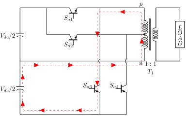
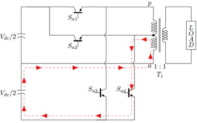
In this paper, a new topology for 3-phase cascaded multilevel inverter is proposed, which overcomes the negative aspects of the existing topologies. In the proposed EC-MLI topology, the power diodes are eliminated which reduces the losses. The proposed topology is shown in Fig. 1 which involves three single-phase five-level inverter represented by, Phase A, B and C, which is coupled by Primary Center Tapped-Three Phase Transformer (PCT-TPT). The individual phase of the inverter circuit is structured by four power switches to and two voltage balancing capacitors and ; also, a single DC source is used at the input end of the inverter to produce an AC output voltage. The two capacitors and are coupled in series to split the input voltage into five levels.
Fig. 1Three-phase five-level EC-MLI architecture
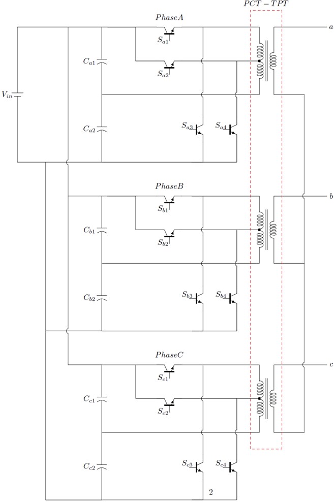
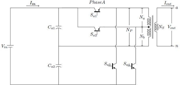
The switches to controls the flow of discharging current to and from the neutral point of capacitors and respectively. Switches to have half of the input voltage as their voltage rating, which is /2. The secondary of the PCT-TPT is star connected. The turn’s ratio / of PCT-TPT winding is : 1:1 to produce five output voltage levels, namely, /2, , 0, –/2, – at the output terminals of the PCT-TPT. For easy understanding, a single phase system is selected for discussion as shown in Fig. 2. To get two equal primary voltages, the tipping point of the center tapped transformer is exactly at the center. The turn's ratio determines the output voltage across the secondary winding (), but power in each winding is the same. Due to the center tap point, the primary winding () is split into two separate circuits. The upper winding is referred to as () and the lower winding as (). The output voltage and current of the single-phase transformer are represented as and respectively. The DC input is switched and given an AC input to the transformer. The voltage and current are represented by and respectively.
Fig. 2Single-phase five-level enhanced cascaded MLI
The input and the output voltages and currents of the transformer are related by the Eq. (1) and Eq. (2) respectively:
Also, the dc input and are applied to either the upper or lower primary winding of the transformer which is represented as or respectively. With the primary center tapped transformer, the input and the output voltage are related to the turns ratio as expressed in Eq. (3) and Eq. (4):
where:
The following are the switch positions to produce the five-level output voltage using the EC-MLI topology. Below mentioned are the switch positions for Phase A:
• To generate an output voltage of (/2), turn on switch .
• To generate an output voltage of (), turn on switch .
• To generate an output voltage of ( 0), turn off all power switches to .
• To generate an output voltage level (/2), turn on switch .
• To generate an output voltage level (), turn on switch .
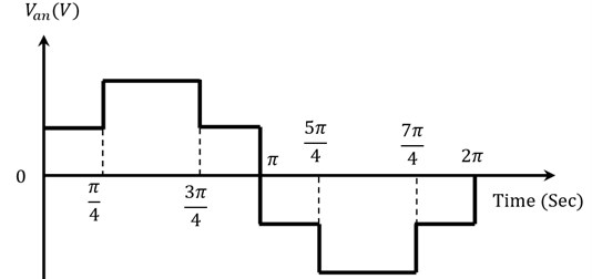
The working principle of the proposed topology along with the conduction path for the five levels of operation is presented in Fig. 3. The voltage at the output of EC-MLI for a complete switching period, from 0 to 2 for one phase (Phase A) is shown in Fig. 4, and the voltage magnitude is represented as .
The output voltage and current are given by Eq. (5) and Eq. (6) respectively:
Fig. 3Working principle of the proposed topology: a) path for output voltage =+Vdc/2, b) path for output voltage =+Vdc/4, c) path for output voltage =-Vdc/2, d) path for output voltage =-Vdc/4
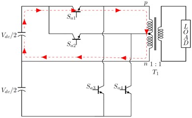
a)
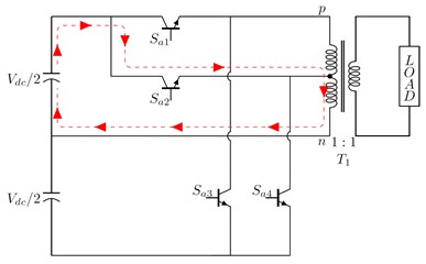
b)
c)
d)
3. Control strategy for the proposed topology
Now, in order to generate the required multilevel output voltage for different time intervals with the available DC voltage, the switches to has to be turned ON and OFF precisely. To generate the desired first output voltage with fewer distortions, proper switching techniques has to be incorporated. The traditional method to generate gating pulses to the power switches is Pulse Width Modulation (PWM) technique. There are two types of high-frequency switching PWM techniques, namely Space Vector PWM and Sinusoidal PWM. Among the two, Space vector pulse width modulation (SVPWM) has the following features: better harmonic quality extended the linear range of operation [18] and good utilization of DC link voltage.
Fig. 4Five-level output voltage
Multicarrier techniques have been proposed in many kinds of literature which reduce the distortions in the output of the multilevel inverter. Here, the unipolar multicarrier SVPWM method is proposed for a 3-phase five-level EC-MLI, due to its pros like less switching losses and also produces low electromagnetic interference [19]. In this modulation technique, a Unipolar Space Vector Reference (USVR) signal with triangular multicarrier waves is used to generate a gating signal for an EC-MLI. In the unipolar triangular multi-carrier technique, we require (-1)/2 triangular carriers with the same frequency and equal amplitude to generate an -level inverter output.
Fig. 5 shows the switching pattern and gating pulses adopted for the proposed EC-MLI. Each triangular wave and the generated USVR is continuously compared to generate the gating signals. If the amplitude of the USVR wave exceeds the amplitude of the triangle carrier, then the corresponding switches are turned on. Else, the switches are turned off. From Fig. 5, it is observed that USVR wave is compared with the respective carriers which generate the signals and . These signals are used to generate the gating signals to , by the phase angle displacement. The switching patterns of the proposed multilevel inverter are represented in terms of logical NOT, AND, OR gates from Eq. (7) through (10):
where to represents an operational interval of switching strategies shown in Fig. 5.
To generate the USVR wave, the 3-phase balanced sinusoidal quantities are transformed to their equivalent two-phase quantities in stationary reference frame using the Clarke transformation. Then the vector magnitude and angle of the two-phase quantities are calculated and used for modulating the inverter output Eq. (20).
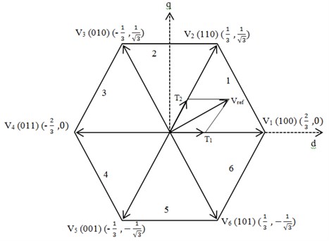
Fig. 6 shows the space vector where the space phasor of the output voltage stays in each of the positions 1 to 6 for a time interval corresponding to 60° of the fundamental period and jumps to the next position at the end of every 60°. Reference voltage vector () derived from the vector summation of all three modulating voltages, is rotated in an anti-clockwise direction from one sector to another at a constant angular speed () for steady state operating condition. Moreover, the time taken by to complete one revolution is equal to the fundamental period of the output voltage. Therefore, the calculations of time variables are given in Eq. (11) to (13):
where and sampling period is related to the sampling frequency ().
Fig. 5Switching pattern and gate pulses for single-phase EC-MLI
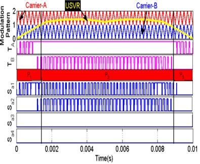
a) Positive cycle switching pattern
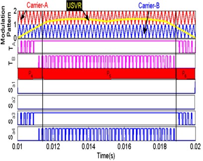
b) Negative cycle switching pattern
Fig. 6Space vector diagram
4. Results and discussions
The 3-phase 5-level EC-MLI is modelled using power system toolbox in SIMULINK. It is configured by three single-phase five-level inverters named as, Phase A, Phase B, and Phase C, which are connected to the load through a PCT-TPT. In this topology, a single DC input is used to which every phase is connected in parallel. The unipolar multicarrier PWM technique is considered here. The proposed switching strategy is based on level shifted multicarrier PWM technique with two carrier signals comparing the USVR signal. In level shifted PWM, the carrier signals are vertically shifted to each other. Few of the level shifted PWM techniques considered for this proposed work are unipolar phase disposition SVPWM (UPD-SVPWM), unipolar phase opposition SVPWM (UPO-SVPWM) and unipolar variable frequency SVPWM (UVF-SVPWM).
4.1. UPD-SVPWM
In Phase Disposition (PD) PWM all the carrier signals will have the same phase. For a five-level EC-MLI, two triangular carriers (i.e., Carrier-A and Carrier-B) which are in phase with each other. Also, both the carriers possess the same frequency 5 kHz and have same amplitude 0 to 1.
To maintain the two carriers in contiguous bands, different offset voltages are used. Modulation pattern for five-level UPD-SVPWM is shown in Fig. 7(a) for a modulation index, = 0.8.
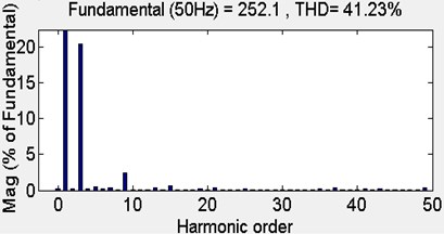
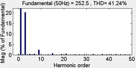
Both the carrier waves are positioned above the zero references. The two carrier waves are compared with the USVR wave to generate the gating signals for the switches to . The synthesized ac output voltages for the three phases are shown in Fig. 7(b)-(d) and its harmonic spectrum is shown in Fig. 8.
Fig. 7Modulation pattern and output voltage with UPD-SVPWM strategy (a)-(d)
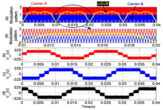
Fig. 8Harmonic spectra with UPD-SVPWM strategy
4.2. UPO-SVPWM
In phase opposition (PO) PWM the carrier signals are out of phase by 180° phase. For a five-level EC-MLI, again two triangular carriers (i.e., Carrier-A and Carrier-B) of same frequency 5 kHz are considered which are out of phase by 180°.
The amplitudes for both the carriers are the same, with 0 to 1. Since both the carriers are preferred to be in adjacent bands, different offset voltages are used. Modulation pattern for five-level UPO-SVPWM is shown in Fig. 9(a) for a modulation index of 0.8. The synthesized ac output voltage for the three phases are shown in Fig. 9(b)-(d). The harmonic spectrum is shown in Fig. 10.
Fig. 9Modulation pattern and output voltage with UPD-SVPWM strategy (a)-(d)
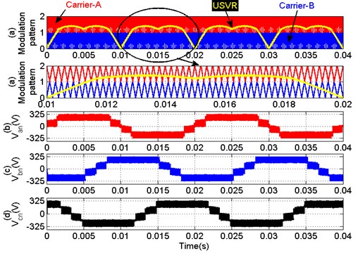
Fig. 10Modulation pattern and output voltage with UPO-SVPWM strategy
4.3. UVF-SVPWM
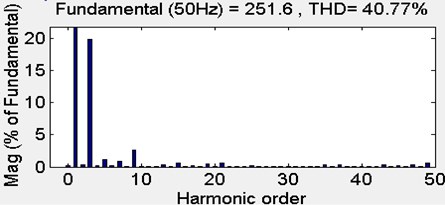
For a five-level EC-MLI, two triangular carriers (i.e., Carrier-A and Carrier-B) with the different frequency 5 kHz and 10 kHz are considered, and the same amplitude 0 to 1 is used. Contiguous bands are occupied with different offset voltages. Modulation patterns using the five-level UVF-SVPWM are presented in Fig. 11(a) for 0.8. The synthesized ac output voltage and the Total Harmonic Distortion is shown in Fig. 12.
5. Performance comparison
For the proposed multilevel inverter various PWM switching techniques were applied and simulation was done using the Simulink power System tool. The performance of different methods like UPD-SVPWM, UPO-SVPWM, and UVF-SVPWM at the modulation index of 0.8 in the context of Total Harmonic Distortion is measured and compared using FFT block, and their values are shown in Table 1 along with the Distortion Factor (DF) and Crest Factor (CF). The expression for Distortion Factor (DF) and Crest Factor (CF) is expressed in Eq. (14) and Eq. (15) respectively. Also, Table 2 shows the peak voltage of inverter output and the THD for various modulation indices. When the modulation index is nearing unity, the THD decreases and the peak output voltage of the inverter increases:
Compared to all the PWM methods, it is inferred that UVF-SVPWM method provides low THD. The peak voltage of inverter output, DF and CF are almost same for all the PWM methods. The THD and peak voltage of inverter output is studied using the FFT block for different values of modulation index ranging from 0.4 to 1, and the corresponding values are shown in Table 2. It is evident that the UVF-SVPWM method provides lower THD and better fundamental peak voltage when the modulation index is nearing unity.
Fig. 11Modulation pattern and output voltage with UPD-SVPWM strategy (a)-(d)
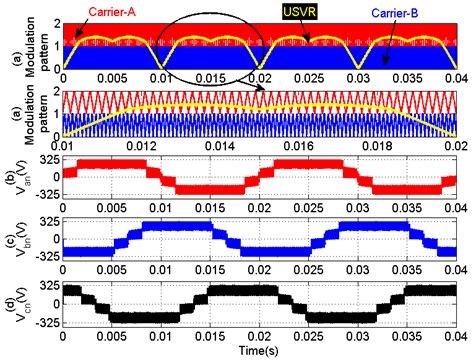
Fig. 12Modulation pattern and output voltage with UVF-SVPWM strategy
All switches required in the proposed topology are bi-directional conducting and unidirectional blocking, the instantaneous conduction and power losses are given by Eq. (16) to (21):
where is the voltage drop in ON state of the diode, is the internal resistance of the diode, is the current flowing through the diode. The average conduction loss is given by:
where is the number of conducting diodes is the load current.
Power loss in the capacitor is negligible and varies based on the switching frequency of the converter. The switching losses are calculated using ON and OFF time period. The energy loss during ON time period is:
where is the loss during ON time period of the th switch, is the turn ON time period, is the current through the switch after switching ON, is the voltage across the switch. Similarly, the energy loss in the OFF time period is calculated as:
where is the turn OFF time of the th switch, is the current through the switch before turning OFF. The power loss in switches is given by:
where represents the number of transitions made by the th switch and the current for switching is same as before and after switching. The total inverter losses are given by [23]:
Table 1Power quality indices for various PWM schemes
Modulation strategy 0.8 | Order of harmonics | DDF | Voltage in PEAK | CCF | ||||||
3rd | 5th | 7th | 9th | 11th | 13th | THD % | ||||
UPD-SVPWM | 20.33 | 0.52 | 0.37 | 2.37 | 0.11 | 0.32 | 41.23 | 0.024 | 252.1 | 1.415 |
UPO-SVPWM | 20.26 | 0.38 | 0.52 | 2.34 | 0.05 | 0.22 | 41.24 | 0.024 | 252.5 | 1.414 |
UVF-SVPWM | 19.88 | 1.09 | 0.88 | 2.69 | 0.01 | 0.36 | 40.77 | 0.025 | 251.6 | 1.414 |
Table 2Power quality indices for various modulation indices
UPD-SVPWM | UPO-SVPWM | UVF-SVPWM | ||||||
THD % | () | THD % | () | THD % | () | |||
0.4 | 84.68 | 123.6 | 0.4 | 84.68 | 123.6 | 0.4 | 87.18 | 116.5 |
0.6 | 38.41 | 189.1 | 0.6 | 38.43 | 189.1 | 0.6 | 38.17 | 185.7 |
0.8 | 41.23 | 252.1 | 0.8 | 41.24 | 252.5 | 0.8 | 40.77 | 251.6 |
1.0 | 36.56 | 317.7 | 1.0 | 36.54 | 317.2 | 1.0 | 36.21 | 317.1 |
In this paper, the proposed 3-phase EC-MLI produces five output levels. To generate five output levels with the existing multilevel inverters like DC-MLI, FC-MLI, CHB-MLI, IC-MLI and ICA-MLI, the component requirement is more when compared to the proposed topology as given in Table 3.
From Table 3, the performance comparison of the proposed system with existing literatures was carried out with respect to the source parameters and the performance parameters. The proposed system has better efficiency, lesser switching losses and the total harmonic distortion is also reduced. We can observe that the DC-MLI and FC-MLI require (–2)×(–3)×3 number of clamping diodes and clamping capacitors excluding the balancing capacitors in the latter case, to generate -level outputs respectively. A CHB-MLI requires (–3)×3 number of independent DC sources. The basic three topologies like DC-MLI, FC-MLI and CHB-MLI needs (–1)×(–3)×3 number of switches. These topologies need an enormous number of components, and so they are not advisable for applications requiring high power/voltage. An IC-MLI requires only one DC source, (–1)×(–3)×3 number of switches and (–2)×2 output transformers. An ICA-MLI needs [(–1)+1]×3 number of switches and (–2) output transformers. These two topologies have minimum power devices compared with the basic topologies. The proposed method is more advantageous as for as the switch count and cost is considered and the system size is less when compared with the conventional approaches. Also, the complete elimination of diodes is achieved.
Table 3Components comparison with existing MLI
MLI parameters | DC-MLI | FC-MLI | CHB-MLI | IC-MLI | ICA-MLI | Proposed MLI |
Literature | (21) | (22) | (23) | (24) | (25) | |
Source parameters | ||||||
Number of switches | 24 | 24 | 24 | 24 | 15 | 12 |
Number of input sources | 1 | 1 | 6 | 1 | 1 | 1 |
Number of capacitors | 4 | 22 | 0 | 0 | 2 | 6 |
Number of diodes | 18 | 0 | 0 | 0 | 12 | 0 |
Number of output transformers | 1 | 1 | 1 | 6 | 3 | 3 |
Performance parameters | ||||||
THD without filter | 43.9 % | 29.5 % | 40.8 % | 35.1 % | 31.7 | 36.2 |
Efficiency | 67.9 | 76.6 % | 72 % | 73.6 % | 72.3 % | 77.8 % |
Switching losses () | 36.82 | 22.69 | 28.43 | 30.31 | 26.28 | 21.76 |
Reactive power support | No | Yes | No | Yes | Yes | Yes |
6. Conclusions
A new five-level inverter was proposed with possible minimum switch count. The working principle of the proposed multilevel inverter was discussed. This topology uses only four switches and one transformer to produce the five-level inverter output. Moreover, the usage of diodes is eliminated which reduces the conduction losses in the system. Also, using MATLAB SIMULINK power system toolbox, the proposed topology was simulated with various multicarrier SVPWM switching techniques like the UPD-SVPWM, UPO-SVPWM, and UVF-SVPWM. The THD, Distortion factor, Crest factor, and Peak voltages were observed for different values of modulation index varying from 0.4 to 1. The results show that when the modulation index nears the unity the peak output voltage of the inverter increases and the THD decreases better in the case of UVF-SVPWM. Since the switch count is less, the cost and system size is reduced when compared with the traditional techniques.
References
-
Mahrous Ahmed E., Saad Mekhilef Design and implementation of a multi-level three-phase inverter with fewer switches and low output voltage distortion. Journal of Power Electronics, Vol. 9, Issue 4, 2009, p. 593-603.
-
Yuan Xiaoming, Barbi Ivo Fundamentals of a new diode clamping multilevel inverter. IEEE Transactions on Power Electronics, Vol. 15, Issue 4, 2000, p. 711-718.
-
Rodriguez J., Lai Jih Sheng, Peng Fang Zheng Multilevel inverters: a survey of topologies, controls, and applications. IEEE Transactions on Industrial Electronics, Vol. 49, Issue 4, 2002, p. 724-738.
-
Raghavendra Reddy Karasani, Vijay Bhanuji Borghate, Prafullachandra M.Meshram, Hiralal Murlidhar Suryawanshi, Sidharth Sabyasachi A three-phase hybrid cascaded modular multilevel inverter for renewable energy environment. IEEE Transactions on Power Electronics, Vol. 32, Issue 2, 2017, p. 1070-1087.
-
Pan Zhiguo, Peng Fang Zheng, Corzinek A., Stefanovicv R., Leuthenj M., Gataric S. Voltage balancing control of diode-clamped multilevel rectifier/inverter systems. IEEE Transactions on Industry Applications, Vol. 41, Issue 6, 2005, p. 1698-1706.
-
Chen Bin, Yao Wenxi, Lu Zhengyu Novel five-level three-phase hybrid-clamped converter with reduced component. Journal of Power Electronics, Vol. 14, Issue 6, 2014, p. 1119-1129.
-
Marchesoni M., Tenca P. Diode-clamped multilevel converters: a practical way to balance DC-link voltages. IEEE Transactions on Industrial Electronics, Vol. 49, Issue 4, 2002, p. 752-765.
-
Anshuman Shukla, Arindam Ghosh, Avinash Joshi Improved multilevel hysteresis current regulation and capacitor voltage balancing schemes for flying capacitor multilevel inverter. IEEE Transactions on Industrial Electronics, Vol. 63, Issue 12, 2016, p. 7814-7822.
-
Reza Barzegarkhoo, Elyas Zamiri, Naser Vosoughi, Hossein Madadi Kojabadi, Liuchen Chang Cascaded multilevel inverter using the series connection of novel capacitor-based units with minimum switch count. IET Power Electronics, Vol. 9, Issue 10, 2016, p. 2060-2075.
-
Soundar Rajan Ponnusamy, Manoharan Subramaniam, Gerald Christopher Raj Irudayaraj, Kaliamoorthy Mylsamy An improved switching topology for single phase multilevel inverter with capacitor voltage balancing technique. Journal of Power Electronics, Vol. 17, Issue 1, 2017, p. 115-126.
-
Rech C., Pinheiro J. R. Hybrid multilevel converters: unified analysis and design considerations. IEEE Transactions on Industrial Electronics, Vol. 54, Issue 2, 2007, p. 1092-1104.
-
Tan G., Deng Q., Liu Z. An optimized SVPWM strategy for five-level active NPC (5L-ANPC) converter. IEEE Transactions on Power Electronics., Vol. 29, Issue 1, 2014, p. 386-395.
-
Song Sung Geun, Kang Feel Soon, Park Sung Jun Cascaded multilevel inverter employing three-phase transformers and single DC input. IEEE Transactions on Industrial Electronics, Vol. 56, Issue 6, 2009, p. 2005-2014.
-
Park Sung Jun, Kang Feel Soon, Lee Man Hyung, Kim Cheul U. A new single-phase five-level PWM inverter employing a deadbeat control scheme. IEEE Transactions on Power Electronics, Vol. 18, Issue 3, 2003, p. 831-843.
-
Daher Sergio, Schmid Jurgen, Antunes Fernando L. M. multilevel inverter topologies for stand-alone PV systems. IEEE Transactions on Industrial Electronics, Vol. 55, Issue 7, 2008, p. 2703-2712.
-
Hajizadeh Mehdi, Fathi Seyed Hamid Fundamental frequency switching strategy for grid-connected cascaded H-bridge multilevel inverter to mitigate voltage harmonics at the point of common coupling. IET Power Electronics, Vol. 9, Issue 12, 2016, p. 2387-2393.
-
Law Kah Haw, Mohamed Dahidah S. A., Haider A. F. Almurib SHE-PWM cascaded multilevel inverter with adjustable DC voltage levels control for STATCOM applications. IEEE Transactions on Power Electronics, Vol. 29, Issue 12, 2014, p. 6433-6444.
-
Matsa A., Ahmed I., Chaudhari M. A. Optimized space vector pulse-width modulation technique for a five-level cascaded H-bridge inverter. Journal of Power Electronics, Vol. 14, Issue 5, 2014, p. 937-945.
-
Rajesh Gupta, Arindam Ghosh, Avinash Joshi Switching characterization of cascaded multilevel-inverter-controlled systems. IEEE Transactions on Industrial Electronics, Vol. 55, Issue 3, 2008, p. 1047-1058.
-
Subash Kumar C. S., Gopalakrishnan V. Design of synchronous reference frame based harmonic detection and space vector pulse width modulation based switching of shunt active filter. Australian Journal of Electrical and Electronics Engineering, Vol. 10, Issue 3, 2013, p. 362-370.
-
Khalili T., Raihani A., Ouajji H., Bouattane O., Amri F. Efficient choice of a multilevel inverter for integration on a hybrid wind-solar power station. Journal of Power and Energy Engineering, Vol. 3, 2015, p. 9-44.
-
Panda A. K., Suresh Y. Research on cascade multilevel inverter with a single DC source by using three-phase transformers. International Journal of Electrical Power and Energy Systems, Vol. 40, Issue 1, 2012, p. 9-20.
-
Song S. G., Kang F. S., Park S.-J. Cascaded multilevel inverter employing three-phase transformers and single DC input. IEEE Transactions on Industrial Electronics, Vol. 56, Issue 6, 2009, p. 2005-2014.
-
Gupta K. K., Jain S. A novel multilevel inverter based on switched DC sources. IEEE Transactions on Industrial Electronics, Vol. 61, Issue 7, 2014, p. 3269-3278.
-
Suresh Y., Venkataramanaiah J., Panda A. K., Dhanamjayulu C., Venugopal P. Investigation on cascade multilevel inverter with symmetric, asymmetric, hybrid and multi-cell configurations. Ain Shams Engineering Journal, Vol. 8, Issue 2, 2017, p. 263-276.
About this article

