Abstract
A flyback topology has advantages like simplicity, better reliability and low cost, but comes with voltage stresses on semiconductor switches caused by the transformer leakage inductance. An improved regenerative snubber has been proposed to meet ever growing demand for higher efficiency. The proposed snubber topology is a modified LCD flying capacitor snubber and has advantages over conventional prototypes promising high efficiency of leakage energy recovery in high power applications. The beneficial features include: reduced circulating currents in snubber circuits; reduced current RMS on the secondary side; the possibility of recovering part of the leakage energy directly to the secondary output. The operation of the proposed snubber is analyzed to reveal benefits and simulation results are presented to verify performance. The stage by stage analysis with governing formulas has been provided. Design considerations are discussed.
1. Introduction
The flyback topology is widely used in low power converter designs due to low component count and, as a result, the simple schematics and a low cost. Also, the topology has gained the fame for excellent robustness, reliability and the possibility to provide galvanic isolation at a relatively low charge. Moreover, improvements in power semiconductors and magnetic components make the flyback topology more efficient and attractive in a variety of low and middle power SMPS applications. Since the topology contributes to the steady growth of the power electronics industry, it is highly desirable to find solutions for efficiency improvement and lifting power boundaries of topology applications. One of the major challenges encountered here by designers is the mitigation of voltage stresses across semiconductor switches caused by the leakage inductance of a flyback transformer. For better efficiency these voltage stresses have to be suppressed by implementing a non-dissipative clamp, preferably the most efficient and passive one to maintain low cost.
Several solutions were proposed to limit voltage spikes across a main switch with the ability to recover leakage energy of a flyback transformer.
Active clamp snubbers with regenerative capabilities are well known in a scientific literature [1-5]. Active clamp can help effectively recover transformer leakage energy; it can also help to provide zero voltage switching for the main power transistor [3-5]. But all of these benefits come with the complexity of active clamping. In addition, an active clamp reduces the robustness of a flyback topology, because the auxiliary clamp switch commutates the snubber capacitor to the output capacitor via the leakage inductance of a small value.
Also, there are some snubbers [6, 7] with a quiet straight forward idea involving commutation of the clamp capacitor to the input to recover stored transformer leakage energy. Snubber in [7] is semi-active and embodies an additional auxiliary switch, which synchronously with the flyback main switch commutates the clamp capacitor to an input through an auxiliary inductor. These said snubbers are featured with a complex structure, but do not compromise the robustness of the flyback topology.
There is also a number of passive non-dissipative snubber circuits for a flyback converter [8-15], known as LCD snubbers, the general circuit is in Fig. 1. It is reported that these passive snubbers reduce turn off switching losses and effectively regenerate leakage energy from a snubber capacitor.
The auxiliary flying capacitor in Fig. 1 resonantly charges and recharges to peak voltages of opposite polarities, therefore, there are additional circulating currents in snubber circuits, which cause an extra power dissipation in snubber diodes and the snubber inductor . The conduction time of the output diode Do is reduced, because when the main transistor , opens, it takes some time to recharge the clamp capacitor before transformer reset [15]. This increases the RMS value on the secondary side.
There are versions of regenerative circuits [12-15], in which the snubber inductor in Fig. 1 is integrated on the same magnetic core as the main transformer. That offers the advantage of reducing the component count. Other advantage of the passive integrated regenerative snubber is that it recovers part of transformer leakage energy back into the transformer magnetizing inductor during the conduction time of a main switch. Therefore, it has reduced current RMS in snubber circuits and the current on the secondary side ramps up faster. It was reported [14] that the integrated regenerative snubbers demonstrate better efficiency than their counterparts.
Fig. 1A flyback converter with conventional lossless LCD snubber
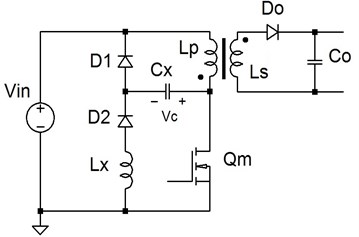
In integrated and non-integrated versions of the LCD snubber, the peak voltage of the snubber capacitor depends on a value of the capacitor and the transformer leakage energy. The bigger the value of the capacitor the smaller the voltage spike will be across the main transistor . But this comes at the expense of higher values of circulating currents and the less conduction time of a flyback secondary side, thus higher RMS and power losses.
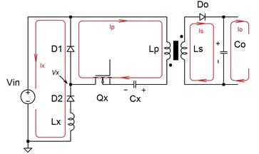
In this paper a novel regenerative semi-active snubber circuit is proposed, which is the subject of a patent application [16]. In Fig. 2 the said snubber is a modified LCD flying capacitor snubber featured with reduced circulating currents, improved current RMS on the secondary side and the ability to maintain a programmable voltage stress across a main power switch.
Fig. 2A flyback converter with the proposed regenerative LCD snubber
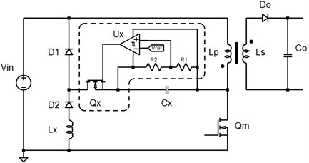
In addition, snubber efficiency could be better if the conduction current of the auxiliary inductor is continues. With extended conduction time for the auxiliary inductor, the snubber could recover part of the leakage energy directly to the secondary output. In Fig. 2 the inductor can be separate or integrated with the main flyback transformer. The integrated version of the proposed snubber recovers part of the leakage energy to the secondary side and stores part of the leakage energy in the magnetizing inductor of the main transformer. With continues conduction current of , the switching losses of the auxiliary diode are reduced to zero. Based on the foregoing, the proposed snubber has the potential to recover flyback transformer leakage energy with higher efficiency. The snubbers’ comparison summary is given on Table 1.
Table 1The summary comparison table of snubbers.
Snubber type | Recovery efficiency | Robustness | Complexity | Power range |
Dissipative RCD | Bad | Best | Simplest | Small power |
Active clamp | Good | Bad | Complex | High power |
DC/DC converter | Good | Good | Most complex | High power |
Regenerative LCD | Good | Best | Simple | Middle power |
Proposed snubber | Good | Good | Less complex | High power |
Only a non-integrated version of the proposed snubber is considered in the current work. To reveal the advantages of the proposed solution, a stage-by-stage consideration has been given and equivalent schematics have been provided for each stage where necessary. Simulation results have been presented to confirm the snubber performance.
2. The proposed semi-active regenerative LCD snubber circuit
In Fig. 2 one can see the voltage limiter embodying the clamp capacitor , the clamp diode , the auxiliary diode and the auxiliary inductor , which helps to recover the energy temporarily stored in the clamp capacitor. Also, here one can see the auxiliary switch with a driving circuitry designed to turn on and turn off the switch at certain voltage levels across the auxiliary capacitor . The behavior of the proposed snubber depends on the specific implementation and multiple parameters. One of the promising recover strategies has been analyzed, in which the comparator prevents the snubber capacitor from excessive discharge. This way the strategy eliminates circulating currents in snubber circuits. Within this strategy, the proposed snubber operates in semi-active mode or some passive modes depending on an input voltage and a flyback output load.
The study was done for a flyback operating in discontinues conduction mode (DCM) while the auxiliary switch in semi-active mode and a snubber inductor current is continues. The DCM mode is characterized by – the time interval when the main flyback switch conducts, – the interval when the main switch is turned off, and – the time the main transformer discharges into the secondary output. One could transit to flyback continues conduction mode (CCM) approaching to zero (). We suggest to start the study of the schematic in Fig. 2 given that all semiconductor switches are ideal. There would be five flyback operation stages to consider.
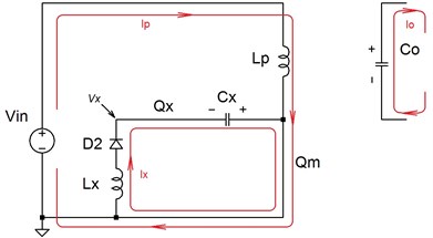
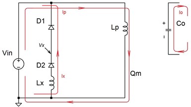
The equivalent circuit schematics are given in Fig. 3 for each of five stages.
The flyback back topology is well known and studied. So the conduction time and the discharge time are related to each other by the Eq. (1):
where – the transformer turns ratio, – the secondary output voltage. During the non-conducting stage of the main switch , the reflected voltage on the primary side is:
Fig. 3Equivalent circuits of operational stages: a) Stage 1; b) Stage 2; c) Stage 3; d) Stage 4; e) Stage 5. On the figures (a-e): Vx – the potential of the D2 cathode; Lp – inductance of transformer primary winding; Ls –inductance of transformer secondary winding; Vin – input voltage; Ip – transformer primary current; Is – transformer secondary current; Ix – the current on the auxiliary inductor Lx; Io – output load current
a)
b)
c)
d)
e)
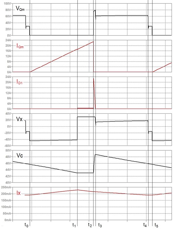
Eq. (1) and Eq. (2) are also correct for a flyback operating in CCM. In this analysis the main attention will paid for the functioning of the proposed snubber. The waveforms in steady state condition have been generated in the LTspice simulation software. To be specific and in case if one wants to simulate and compare results, the circuit parameters are: 10 uH is the transformer primary winding magnetizing inductance, 7 is the turns ratio, 0.992 is the coupling coefficient between primary and secondary windings; the switching frequency is about 64.9 kHz is; 29 V is the input voltage, 210 V is the output voltage, 133.6 W is the output power; 5.6 mH is the snubber inductor. These parameters are common for a solar microinverter flyback, which is the ultimate goal of the research. The auxiliary switch turns off when the voltage across is less then 43 V and turns on when the voltage is more than 47 V.
The duration of the stages and simulated operation waveforms are presented in Fig. 4.
In Fig. 4 one can see that in our particular study case the current of the auxiliary inductor flows in a continues conduction manner, the voltage across the capacitor changes slightly, that means there are no circulating currents except for that, which corresponds to the leakage energy pumping into . The main switch turns on at the time moment and the hole switching cycle lasts from the moment until the moment t5. By the moment the voltage across the capacitor is higher than the upper threshold 47 V, that causes the trigger to hold the auxiliary switch turned on.
Fig. 4Simulation waveforms of the flyback converter circuit with the proposed regenerative snubber: VQm – drain to source voltage on the switch Qm; IQm – the current of the switch Qm; ID1 – the current of the clamping diode D1; Vx – the potential of the D2 cathode; Vc – the voltage on clamp capacitor Cx; Ix – the current on the auxiliary inductor Lx
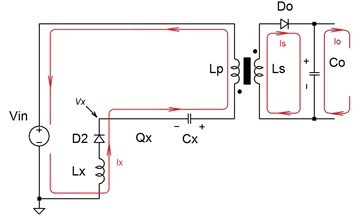
2.1. Stage 1 ()
At this stage, see Fig. 2, the main switch is turned on, the transformer primary side is connected to the input mains Vin and the transformer starts to gain power. The equivalent schematic of this stage is presented in Fig. 3(a), where the schematic components that are not engaged are not shown in the figure. The transformer secondary side does not provide any current, and the load current is supplied by the output capacitor . The auxiliary diode remains non-conducting. The transformer current on the primary side is increasing linearly by time. At this stage the auxiliary switch is conducting because the voltage of the capacitor is higher than the closing threshold 43 V of the trigger . The current of the auxiliary inductor also increases steadily, because the snubber capacitor is now applied to via the main switch . This stage lasts until the voltage across drops to 43 V, at which point the auxiliary transistor turns off. Let be the steady state voltage across , then during this stage will increase by the value:
where , . The auxiliary diode is reversed biased by the voltage .
2.2. Stage 2 ()
By the moment the voltage of the snubber capacitor has dropped to low threshold 43 V, therefore the auxiliary switch has been turned off. This prevents the capacitor from deep discharge and thus eliminates circulating currents unrelated to the leakage recovery. The auxiliary inductor current is now redirected to charge the input supply through the diode , thus the potential in Fig. 4 rises to an input value . The main transformer still gains power. The inductor discharges to the input and during this stage its current falls by the value:
where is defined as equal to .
2.3. Stage 3 ()
At the moment the main switch turns off, see 0 in Fig. 4, and the transformer primary current is redirected and starts charging the clamp capacitor via an internal diode of the auxiliary and the diode D1 until the transformer leakage energy is depleted, what happens by the time moment . At this time interval the equivalent schematic is in Fig. 3(c). During this stage the secondary side current rises from zero. The current continues to discharge to the input for this short period of time. The auxiliary capacitor provides a voltage to reset the main transformer, hence reverses rapidly:
where – the transformer leakage inductance measured from the primary side. , and are the transformer primary winding inductance, the transformer secondary winding inductance and the transformer windings mutual inductance correspondingly. The time duration of this stage can be derived from Eq. (5) and estimated with the help of Eq. (6):
where – the peak of the primary side current before opens, is close to the maximum value of an auxiliary inductor current before opens. Here in Eq. (6) is neglected compared to . The turn-off threshold voltage 43 V and the capacitance value of determine the clamping voltage of the proposed snubber and transformer primary current reverse time .
At this stage the snubber capacitor is charged above the upper threshold voltage of 47 V, set by the comparator , and the snubber transistor is opened again. The upper threshold should be established just over the low threshold 43 V with some margin to exclude false opening of , it is the only guide.
2.4. Stage 4 ()
The equivalent schematic of this stage is in Fig. 3(d). By the moment t3 the transformer leakage energy has been depleted, has dropped to a value equal to the inductor current and the diode has been closed, see 0 in Fig. 4. During this time interval the transformer secondary side discharges the energy gained at stages 1 and 2 into the output capacitor through the diode , namely, the secondary side current decreases. The auxiliary inductor current flows through the auxiliary capacitor and the primary winding , see Fig. 3(d). Therefore, now the snubber inductor and the snubber capacitor recover part of their energy accumulated in previous stages to the input power supply and discharge part of the energy to the main transformer, which in turn recovers it into the secondary output at once. The voltage applied to the inductor equals to . Thus, taking into account Eq. (1) the current change during discharge time is found as:
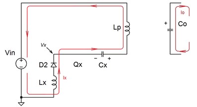
2.5. Stage 5 ()
By the time the secondary current has exhausted, 0, and the last operation stage starts, see Fig. 3(e). The secondary diode Do is reversed, the main switch is still open, hence the flyback enters into a dwell mode. Now the energy of the snubber inductor and the snubber capacitor is recovering into the input only. The voltage applied across the auxiliary inductor and the transformer primary inductor is , therefore at this stage the auxiliary inductor current will change by the value, taking into account that :
where the dwelling time .
3. Discussion
(1) Due to the low discharge current the snubber auxiliary capacitor might not discharge to a low threshold level 43 V by the end of stage 1 and might continue discharge up to stage 3, when the main transistor is opened. It means there will be no stage 2, 0, the snubber switch will be always turned on and the proposed snubber will operate in the passive mode as a conventional LCD snubber. This could happen, for example, if the input voltage rises above the low threshold value 43 V, that causes the snubber capacitor voltage to be equal to 43 V. This case is discussed later.
(2) At light load during stage 3 there might be not enough leakage energy to charge the snubber capacitor to the upper threshold, at which the switch should be turned on. The snubber enters a charge accumulating passive mode. In this mode will be open for a number of switching cycles until the capacitor charges to the upper threshold of 47 V.
(3) If the snubber capacitor prolongs discharge to 43 V threshold up to stage 4, so as the snubber transistor turns off in the middle of stage 4, that does not cause danger to the flyback operation, but it means that the snubber was not optimally designed.
(4) In steady state of the considered semi-active mode the auxiliary inductance current does not change during the full switching cycle of a flyback, 0. Therefore, combining changes in Eq. (3), Eq. (4), Eq. (7) and Eq. (8) of for stages 1, 2, 4 and 5 and neglecting the change in Eq. (5) of during stage 3, because of small value of the primary current reverse time , one could find that:
where – the switching period, from which it is easily found that:
The Eq. (10) has been obtained for a flyback in DCM. As soon as the result is correct for any dwelling time , therefore it is correct for a flyback operating in CCM, keeping in mind that is neglected.
The Eq. (10) establishes dependence of the time interval , during which a snubber capacitor do not discharge, upon the designed voltage level of a clamp capacitor and the given input voltage . Following the analysis, in steady state the clamping voltage could not be set at values lower than the input voltage , and the auxiliary logic with the auxiliary switch will not help. That should be taken into account when designing the snubber. Also, for a successful transformer reset it is desirable for to be higher than the transformer voltage reflected on the primary side, in Eq. (2), so as:
The same conclusions are true for a flyback operating in CCM, except for the fact that there will be no dwelling stage 5 as in case of flyback DCM.
(5) First, if being charged to almost the constant voltage according to Eq. (11), the snubber capacitor captures only transformer leakage energy, and there will be no stray circulating currents caused by the flying capacitor recharge. This results in reduced losses of the recovered leakage energy, eased requirements for snubber components concerning peak current capability and power dissipation.
The second advantage of the proposed snubber circuit over conventional non-integrated and integrated LCD regenerative snubbers is that the secondary current rises without delay as it does in conventional snubbers due to flying capacitor recharge. This reduces RMS on the flyback secondary side.
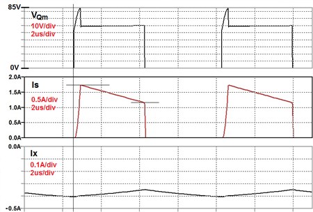
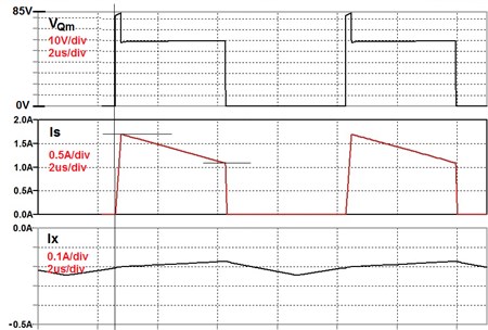
In Fig. 5 one can see the simulation waveforms for the flyback in CCM with the output power 135 W, the output load 330 Ohm and the input voltage 30 V.
The Fig. 5(a) relates to a flyback with a traditional non-integrated LCD snubber and the Fig. 5(b) relates to a flyback with the proposed non-integrated regenerative snubber. Here, the transformer magnetizing inductance was chosen to be 50 uH for the implementation of flyback CCM, the auxiliary inductance is 3 mH. From these waveforms one can notice that with 3 mH the auxiliary inductor current is continues for both proposed and traditional snubbers. In the proposed snubber is about 200 mA. The auxiliary inductor current in case of the traditional snubber is two times larger than in case of the proposed snubber. This is the evidence of decreased circulating currents in the proposed snubber.
Fig. 5Comparative simulation waveforms: a) traditional non-integrated LCD snubber; b) proposed non-integrated regenerative snubber. On figures (a, b): VQm – drain to source voltage on the switch Qm, Is – current of the secondary side diode Do, Ix – current of the auxiliary inductor Lx
a)
b)
In Fig. 5(b) it is seen that the voltage spike across the main switch equals to 85 V with the voltage pulse across an auxiliary capacitor. A value of the capacitor 180 nF of the conventional snubber was chosen to cause the same voltage spike about 85 V across the main flyback switch, see Fig. 5(a). Comparing Fig. 5(a) with Fig. 5(b) one can see, that the secondary side conducting time is reduced with the conventional snubber due to the delayed current start, therefore the secondary current RMS is increased, what impairs efficiency.
Third, the current might be continues in an auxiliary inductor to reduce RMS further, eliminate switching losses of the auxiliary diode D2 and more. For example, in the considered study case part of the leakage energy captured at transformer reset stage 3 is recycled at stage 4 forward to the output through the transformer, adding to a potential efficiency improvement. This is the consequence of the prolonged conduction of the snubber inductor current Ix.
(6) Summing up, the proposed snubber has the potential to recover transformer leakage energy with higher efficiency than the conventional one shown in Fig. 1. The drawback is that the proposed solution requires an additional auxiliary switch and a logic circuit, although the idea behind the logic is quiet simple. The auxiliary transistor conducts and switches the inductor current Ix of a small value, hence one might expect no sufficient negative influence on the leakage recovery efficiency. Therefore, this solution is justified and effective in high power converters. To maintain high recovery efficiency the comparator of an auxiliary logic might be a low or ultra-low power device, which is available on the market at a reasonable price.
(7) Up to this moment the proposed snubber acting in semi-active mode was considered, but at a high input voltage or light load conditions or whenever Eq. (12) is true, the snubber might also operate at the passive mode with the ever turned auxiliary switch :
Therefore, one can put the time 0 in Eq. (10) and get that in this mode , meaning that the auxiliary capacitor voltage will follow the input voltage. And because of Eq. (12) the snubber capacitor voltage still meets the level requirement of Eq. (11) preferable to keep circulating currents low.
(8) An auxiliary inductor current does not resonate with an auxiliary capacitor in the proposed snubber. To keep low power losses in snubber circuits it is preferable to maintain the current ripple of an auxiliary inductor at moderate values, comparable to or lower than the auxiliary inductor average current. This means, the auxiliary inductor current has to be continues for better efficiency or smaller inductor size of the snubber.
Let us evaluate the mean value of the auxiliary inductor current . The snubber clamp receives the leakage energy of a transformer at stage 3:
Then the clamp capacitor gets rid off the energy gained. In stage 1:
In stage 2:
In stage 4:
In stage 5:
Then combining energy changes Eqs. (13-17) altogether and neglecting time, one gets:
4. Conclusions
A novel semi-active regenerative snubber was proposed in the paper. Advantages of the snubber were revealed in stage-by-stage analysis with reference to verifying simulation waveforms. The snubber design guide and main calculation formulas have been provided. In a future work a laboratory device will be created and experimental results will be presented.
The integration of the snubber auxiliary inductor with the main flyback transformer is possible within the proposed snubber schematic, which opens other potential advantages.
References
-
T. F. Wu, S. A. Liang, C. H. Lee. A family of isolated single-stage ZVS-PWM active-clamping converters. Proceedings of IEEE Power Electronics Specialists Conference, Vol. 2, 1999, p. 665-670.
-
Li Q., Lee F. C. Design consideration of the active-clamp forward converter with current mode control during large-signal transient. Proceedings of IEEE Power Electronics Specialists Conference, Vol. 2, 2000, p. 966-972.
-
Watson R., Lee F. C., Hua G. C. Utilization of an active - clamp circuit to achieve soft switching in flyback converters. IEEE Transactions on Power Electronics, Vol. 11, Issue 1, 1996, p. 162-169.
-
Wu T.-F., Lai Y.-S., Hung J.-C., Y.-M., Chen An improved boost converter with coupled inductors and buck-boost type of active clamp. Proceedings of Industry Applications Conference, 2005, p. 639-644.
-
Tseng S.-Y., Hsieh C.-T., Lin H.-C. Active clamp interleaved flyback converter with single-capacitor turn-off snubber for stunning poultry applications. Proceedings of IEEE Power Electronics and Drive System Conference, 2007, p. 1401-1408.
-
Martine Fornage Method and Apparatus for a Leakage Energy Recovery Circuit. USA Patent, US2009/0225574A1, 2009.
-
Gregory Allen Kern, Tilak Gopalarathnam Power Converter and Methods for Active Leakage Energy Recovery in a Power Converter. USA Patent, US2013/0343098A1, 2013.
-
Ninomiya T., Tanaka T., Harada K. Analysis and optimization of a non dissipative LC turn-off snubber. IEEE Transactions on Power Electronics, Vol. 3, 1988, p. 1147-156.
-
Petkov R., Hobson L. Analysis and optimization of a flyback convertor with a non dissipative snubber. IEE Proceedings on Electric Power Applications, Vol. 142, Issue 1, 1995, p. 35-42.
-
Hirokawa M., Ninomiya T. Non dissipative snubber for rectifying diodes applied to a front-end power supply. Proceedings of IEEE Power conversion conference, Vol. 3, 2002, p. 1176-1181.
-
Liao C., Smedley K. Design of high efficiency flyback converter with energy regenerative snubber. Proceedings on IEEE Applied Power Electronics Conference and Exposition, 2008.
-
Jinrong Qian, Da Feng Weng Leakage Energy Recovering System and Method for Flyback Converter. USA Patent, US6473318, 2002.
-
Qian Jinrong, Weng Da F. Voltage Clamping System and Method for a Dc/Dc Converter. World Intellectual Property Organization, WO02/41479A2, 2002.
-
Tsu Hua Ai A novel integrated non dissipative snubber for flyback converter. IEEE International Conference on Systems and Signals, Vol. 2005, 2005, p. 66-71.
-
Abramovitz Alexander Analysis and design of energy regenerative snubber for transformer isolated converters. IEEE Transaction on Power Electronics, Vol. 29, Issue 11, 2014, p. 6030-6040.
-
Dzhunusbekov E. J. Method and Apparatus for a Transformer Leakage Energy Recovery Circuit in a Flyback Converter. Eurasian Patent Organization, EAPO201900050A1, 2020.
About this article

The research was funded by the JSC “Kazakh-British Technical University”, and the Science Committee of the Ministry of Education and Science of the Republic of Kazakhstan.
